BD681 ON Semiconductor, BD681 Datasheet - Page 2
BD681
Manufacturer Part Number
BD681
Description
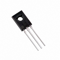
TRANS DARL NPN 4A 100V TO225AA
Manufacturer
ON Semiconductor
Datasheet
1.BD681G.pdf
(4 pages)
Specifications of BD681
Transistor Type
NPN - Darlington
Current - Collector (ic) (max)
4A
Voltage - Collector Emitter Breakdown (max)
100V
Vce Saturation (max) @ Ib, Ic
2.5V @ 30mA, 1.5A
Current - Collector Cutoff (max)
500µA
Dc Current Gain (hfe) (min) @ Ic, Vce
750 @ 1.5A, 3V
Power - Max
40W
Mounting Type
Through Hole
Package / Case
TO-225-3
Lead Free Status / RoHS Status
Contains lead / RoHS non-compliant
Frequency - Transition
-
Other names
BD681OS
Available stocks
Company
Part Number
Manufacturer
Quantity
Price

Company:
Part Number:
BD681
Manufacturer:
STMicroelectronics
Quantity:
1 867
Part Number:
BD681
Manufacturer:
ON/安森美
Quantity:
20 000
Company:
Part Number:
BD681STU
Manufacturer:
FCS
Quantity:
1 981


Î Î Î Î Î Î Î Î Î Î Î Î Î Î Î Î Î Î Î Î Î Î Î Î Î Î Î Î Î Î Î Î Î
Î Î Î Î Î Î Î Î Î Î Î Î Î Î Î Î Î Î Î Î Î Î Î Î Î Î Î Î Î Î Î Î Î
Î Î Î Î Î Î Î Î Î Î Î Î Î Î Î Î Î Î Î Î Î Î Î
Î Î Î Î Î Î Î Î Î Î Î Î Î Î Î Î Î Î Î Î Î Î Î
Î Î Î Î Î Î Î Î Î Î Î Î Î Î Î Î Î Î Î Î Î Î Î Î Î Î Î Î Î Î Î Î Î
Î Î Î Î Î Î Î Î Î Î Î Î Î Î Î Î Î Î Î Î Î Î Î Î Î Î Î Î Î Î Î Î Î
Î Î Î Î Î Î Î Î Î Î Î Î Î Î Î Î Î Î Î Î Î Î Î
Î Î Î Î Î Î Î Î Î Î Î Î Î Î Î Î Î Î Î Î Î Î Î
Î Î Î Î Î Î Î Î Î Î Î Î Î Î Î Î Î Î Î Î Î Î Î
Î Î Î Î Î Î Î Î Î Î Î Î Î Î Î Î Î Î Î Î Î Î Î
Î Î Î Î Î Î Î Î Î Î Î Î Î Î Î Î Î Î Î Î Î Î Î
Î Î Î Î Î Î Î Î Î Î Î Î Î Î Î Î Î Î Î Î Î Î Î
Î Î Î Î Î Î Î Î Î Î Î Î Î Î Î Î Î Î Î Î Î Î Î
Î Î Î Î Î Î Î Î Î Î Î Î Î Î Î Î Î Î Î Î Î Î Î
Î Î Î Î Î Î Î Î Î Î Î Î Î Î Î Î Î Î Î Î Î Î Î
Î Î Î Î Î Î Î Î Î Î Î Î Î Î Î Î Î Î Î Î Î Î Î
Î Î Î Î Î Î Î Î Î Î Î Î Î Î Î Î Î Î Î Î Î Î Î
Î Î Î Î Î Î Î Î Î Î Î Î Î Î Î Î Î Î Î Î Î Î Î Î Î Î Î Î Î Î Î Î Î
Î Î Î Î Î Î Î Î Î Î Î Î Î Î Î Î Î Î Î Î Î Î Î Î Î Î Î Î Î Î Î Î Î
Î Î Î Î Î Î Î Î Î Î Î Î Î Î Î Î Î Î Î Î Î Î Î
Î Î Î Î Î Î Î Î Î Î Î Î Î Î Î Î Î Î Î Î Î Î Î
Î Î Î Î Î Î Î Î Î Î Î Î Î Î Î Î Î Î Î Î Î Î Î
Î Î Î Î Î Î Î Î Î Î Î Î Î Î Î Î Î Î Î Î Î Î Î
Î Î Î Î Î Î Î Î Î Î Î Î Î Î Î Î Î Î Î Î Î Î Î
Î Î Î Î Î Î Î Î Î Î Î Î Î Î Î Î Î Î Î Î Î Î Î
Î Î Î Î Î Î Î Î Î Î Î Î Î Î Î Î Î Î Î Î Î Î Î
Î Î Î Î Î Î Î Î Î Î Î Î Î Î Î Î Î Î Î Î Î Î Î
Î Î Î Î Î Î Î Î Î Î Î Î Î Î Î Î Î Î Î Î Î Î Î
Î Î Î Î Î Î Î Î Î Î Î Î Î Î Î Î Î Î Î Î Î Î Î
Î Î Î Î Î Î Î Î Î Î Î Î Î Î Î Î Î Î Î Î Î Î Î Î Î Î Î Î Î Î Î Î Î
Î Î Î Î Î Î Î Î Î Î Î Î Î Î Î Î Î Î Î Î Î Î Î Î Î Î Î Î Î Î Î Î Î
Î Î Î Î Î Î Î Î Î Î Î Î Î Î Î Î Î Î Î Î Î Î Î
Î Î Î Î Î Î Î Î Î Î Î Î Î Î Î Î Î Î Î Î Î Î Î
1. Pulse Test: Pulse Width v 300 ms, Duty Cycle v 2.0%.
a transistor average junction temperature and secondary
breakdown. Safe operating area curves indicate I
limits of the transistor that must be observed for reliable
operation; e.g., the transistor must not be subjected to greater
dissipation than the curves indicate.
ELECTRICAL CHARACTERISTICS
OFF CHARACTERISTICS
ON CHARACTERISTICS
DYNAMIC CHARACTERISTICS
Collector−Emitter Breakdown Voltage, (Note 1)
Collector Cutoff Current (V
Collector Cutoff Current
Emitter Cutoff Current (V
DC Currert Gain, (Note 1)
Collector−Emitter Saturation Voltage, (Note 1)
Base−Emitter On Voltage, (Note 1)
Small Signal Current Gain (I
There are two limitations on the power handling ability of
(I
(V
(V
(I
(I
(I
(I
(I
(I
5.0
40
10
50
45
35
30
25
20
15
C
C
C
C
C
C
C
0
CB
CB
15
= 50 mAdc, I
= 1.5 Adc,V
= 2.0 Adc, V
= 1.5 Adc, I
= 2.0 Adc, I
= 1.5 Adc, V
= 2.0 Adc, V
= Rated BV
= Rated BV
30
Figure 1. Power Temperature Derating
45
B
B
CE
CE
CE
CE
B
= 30 mAdc)
= 40 mAdc)
CEO
CEO
= 0)
= 3.0 Vdc)
= 3.0 Vdc)
= 3.0 Vdc)
= 3 0 Vdc)
60
T
, I
, I
C
BE
, CASE TEMPERATURE (°C)
E
E
CE
= 0)
= 0, T
75
= 5.0 Vdc, I
C
= Half Rated V
= 1.5 Adc, V
C
90
= 100’C)
Characteristic
C
105
(T
= 0)
C
CE
= 25_C unless otherwise noted)
CEO
120
= 3.0 Vdc, f = 1.0 MHz)
, I
B
135
= 0)
C
150
http://onsemi.com
− V
CE
165
BD675, 677, 679, 681
BD675A, 677A, 679A
BD677, 679, 681
BD675A, 677A, 679A
BD677, 679, 681
BD675A, 677A, 679A
2
the power that can be handled to values less than the
limitations imposed by secondary breakdown.
0.05
BD675, 675A
BD677, 677A
BD679, 679A
BD681
5.0
2.0
1.0
0.5
0.2
0.1
At high case temperatures, thermal limitations will reduce
1.0
T
C
2.0
Figure 2. DC Safe Operating Area
= 25°C
V
CE
, COLLECTOR-EMITTER VOLTAGE (VOLTS)
BONDING WIRE LIMIT
THERMALLY LIMIT at T
SECONDARY BREAKDOWN LIMIT
Î Î Î Î
Î Î Î Î
Î Î Î Î
Î Î Î Î
Î Î Î Î
Î Î Î Î
Î Î Î Î
Î Î Î Î
Î Î Î Î
Î Î Î Î
Î Î Î Î
Î Î Î Î
Î Î Î Î
Î Î Î Î
Î Î Î Î
Î Î Î Î
Î Î Î Î
Î Î Î Î
Î Î Î Î
Î Î Î Î
Î Î Î Î
Î Î Î Î
Î Î Î Î
Î Î Î Î
Î Î Î Î
Symbol
V
V
BV
CE(sat)
I
I
I
BE(on)
CEO
CBO
h
EBO
h
FE
5.0
CEO
fe
Î Î Î
Î Î Î
Î Î Î
Î Î Î
Î Î Î
Î Î Î
Î Î Î
Î Î Î
Î Î Î
Î Î Î
Î Î Î
Î Î Î
Î Î Î
Î Î Î
Î Î Î
Î Î Î
Î Î Î
Î Î Î
Î Î Î
Î Î Î
Î Î Î
Î Î Î
Î Î Î
Î Î Î
Î Î Î
BD675, 675A
BD677, 677A
BD679, 679A
10
Min
100
750
750
1.0
45
60
80
—
C
−
−
−
−
−
−
−
BD681
= 25°C
Î Î Î Î
Î Î Î Î
Î Î Î Î
Î Î Î Î
Î Î Î Î
Î Î Î Î
Î Î Î Î
Î Î Î Î
Î Î Î Î
Î Î Î Î
Î Î Î Î
Î Î Î Î
Î Î Î Î
Î Î Î Î
Î Î Î Î
Î Î Î Î
Î Î Î Î
Î Î Î Î
Î Î Î Î
Î Î Î Î
Î Î Î Î
Î Î Î Î
Î Î Î Î
Î Î Î Î
Î Î Î Î
20
Max
500
0.2
2.0
2.0
2.5
2.8
2.5
2.5
−
−
−
−
−
−
−
Î Î Î
Î Î Î
Î Î Î
Î Î Î
Î Î Î
Î Î Î
Î Î Î
Î Î Î
Î Î Î
Î Î Î
Î Î Î
Î Î Î
Î Î Î
Î Î Î
Î Î Î
Î Î Î
Î Î Î
Î Î Î
Î Î Î
Î Î Î
Î Î Î
Î Î Î
Î Î Î
Î Î Î
Î Î Î
50
mAdc
mAdc
mAdc
Unit
Vdc
Vdc
Vdc
−
−
100
Related parts for BD681
Image
Part Number
Description
Manufacturer
Datasheet
Request
R

Part Number:
Description:
ON Semiconductor [VOLTAGE REGULATOR]
Manufacturer:
ON Semiconductor
Datasheet:
Part Number:
Description:
357-036-542-201 CARDEDGE 36POS DL .156 BLK LOPRO
Manufacturer:
ON Semiconductor
Datasheet:
Part Number:
Description:
357-036-542-201 CARDEDGE 36POS DL .156 BLK LOPRO
Manufacturer:
ON Semiconductor
Datasheet:
Part Number:
Description:
357-036-542-201 CARDEDGE 36POS DL .156 BLK LOPRO
Manufacturer:
ON Semiconductor
Datasheet:
Part Number:
Description:
357-036-542-201 CARDEDGE 36POS DL .156 BLK LOPRO
Manufacturer:
ON Semiconductor
Datasheet:
Part Number:
Description:
357-036-542-201 CARDEDGE 36POS DL .156 BLK LOPRO
Manufacturer:
ON Semiconductor
Datasheet:
Part Number:
Description:
357-036-542-201 CARDEDGE 36POS DL .156 BLK LOPRO
Manufacturer:
ON Semiconductor
Datasheet:
Part Number:
Description:
357-036-542-201 CARDEDGE 36POS DL .156 BLK LOPRO
Manufacturer:
ON Semiconductor
Datasheet:
Part Number:
Description:
357-036-542-201 CARDEDGE 36POS DL .156 BLK LOPRO
Manufacturer:
ON Semiconductor
Datasheet:
Part Number:
Description:
357-036-542-201 CARDEDGE 36POS DL .156 BLK LOPRO
Manufacturer:
ON Semiconductor
Datasheet:
Part Number:
Description:
357-036-542-201 CARDEDGE 36POS DL .156 BLK LOPRO
Manufacturer:
ON Semiconductor
Datasheet:
Part Number:
Description:
Manufacturer:
ON Semiconductor
Datasheet:
Part Number:
Description:
Manufacturer:
ON Semiconductor
Datasheet:
Part Number:
Description:
Manufacturer:
ON Semiconductor
Datasheet: