MJH6287 ON Semiconductor, MJH6287 Datasheet - Page 2
MJH6287
Manufacturer Part Number
MJH6287
Description
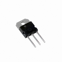
TRANS DARL PNP 20A 100V TO218
Manufacturer
ON Semiconductor
Datasheet
1.MJH6287G.pdf
(5 pages)
Specifications of MJH6287
Transistor Type
PNP - Darlington
Current - Collector (ic) (max)
20A
Voltage - Collector Emitter Breakdown (max)
100V
Vce Saturation (max) @ Ib, Ic
3V @ 200mA, 20A
Current - Collector Cutoff (max)
1mA
Dc Current Gain (hfe) (min) @ Ic, Vce
750 @ 10A, 3V
Power - Max
160W
Frequency - Transition
4MHz
Mounting Type
Through Hole
Package / Case
SOT-93, TO-218 (Straight Leads)
Lead Free Status / RoHS Status
Contains lead / RoHS non-compliant
Other names
MJH6287OS
Available stocks
Company
Part Number
Manufacturer
Quantity
Price

Company:
Part Number:
MJH6287G
Manufacturer:
ON
Quantity:
30 000


1. Pulse test: Pulse Width = 300 ms, Duty Cycle = 2.0%.
ELECTRICAL CHARACTERISTICS
OFF CHARACTERISTICS
ON CHARACTERISTICS (Note 1)
DYNAMIC CHARACTERISTICS
SWITCHING CHARACTERISTICS
Collector-Emitter Sustaining Voltage (I
Collector Cutoff Current (V
Collector Cutoff Current
Emitter Cutoff Current (V
DC Current Gain
Collector-Emitter Saturation Voltage
Base-Emitter On Voltage (I
Base-Emitter Saturation Voltage (I
Current-Gain Bandwidth Product (I
Output Capacitance
Small-Signal Current Gain (I
Delay Time
Rise Time
Storage Time
Fall Time
APPROX
APPROX
R
D
- 8.0 V
+12 V
B
1
, MUST BE FAST RECOVERY TYPES, e.g.:
V2
V1
1N5825 USED ABOVE I
MSD6100 USED BELOW I
& R
(V
(V
(I
(I
(I
(I
(V
C
C
C
C
CE
CE
CB
t
DUTY CYCLE = 1.0%
C
0
r
, t
= 10 Adc, V
= 20 Adc, V
= 10 Adc, I
= 20 Adc, I
VARIED TO OBTAIN DESIRED CURRENT LEVELS
f
, ≤ 10 ns
= Rated V
= Rated V
= 10 Vdc, I
For NPN test circuit reverse diode and voltage polarities.
Figure 2. Switching Times Test Circuit
B
B
CE
CE
CB
CB
= 40 mAdc)
= 200 mAdc)
E
, V
, V
= 0, f = 0.1 MHz)
= 3.0 Vdc)
= 3.0 Vdc)
25 ms
B
V
I
Duty Cycle = 1.0%
≈ 100 mA
BE(off)
BE(off)
B1
B
BE
CC
≈ 100 mA
CE
C
= I
= 5.0 Vdc, I
C
= 30 Vdc, I
= 10 Adc, V
= 50 Vdc, I
B2
= 1.5 Vdc)
= 1.5 Vdc, T
= 10 Adc, V
51
= 100 mA
Resistive Load
Characteristic
C
C
R
D
= 20 Adc, I
B
= 10 Adc, V
+ 4.0 V
1
C
C
C
for t
and V2 = 0
= 0.1 Adc, I
B
CE
= 0)
= 10 Adc
(T
= 0)
CE
C
d
MJH6284 (NPN), MJH6287 (PNP)
C
= 3.0 Vdc)
≈ 8.0 k
and t
= 150_C)
= 25_C unless otherwise noted)
= 3.0 Vdc, f = 1.0 kHz)
B
CE
r
= 200 mAdc)
, D
TUT
B
= 3.0 Vdc, f = 1.0 MHz)
1
≈ 50
is disconnected
= 0)
- 30 V
V
http://onsemi.com
CC
R
C
SCOPE
BASE
2
MJH6284
MJH6287
MJH6284
NPN
Figure 3. Darlington Schematic
COLLECTOR
V
Symbol
Symbol
V
V
V
EMITTER
CEO(sus)
I
I
I
CE(sat)
BE(sat)
BE(on)
h
C
CEO
CEX
EBO
h
f
t
t
FE
t
t
T
ob
d
fe
s
r
f
BASE
NPN
Min
100
750
100
300
4.0
0.1
0.3
1.0
3.5
-
-
-
-
-
-
-
-
-
-
Typical
MJH6287
PNP
18,000
PNP
Max
400
600
1.0
0.5
5.0
2.0
2.0
3.0
2.8
4.0
0.1
0.3
1.0
2.0
-
-
-
-
COLLECTOR
EMITTER
mAdc
mAdc
mAdc
MHz
Unit
Unit
Vdc
Vdc
Vdc
Vdc
pF
ms
-
-
Related parts for MJH6287
Image
Part Number
Description
Manufacturer
Datasheet
Request
R

Part Number:
Description:
ON Semiconductor [VOLTAGE REGULATOR]
Manufacturer:
ON Semiconductor
Datasheet:
Part Number:
Description:
357-036-542-201 CARDEDGE 36POS DL .156 BLK LOPRO
Manufacturer:
ON Semiconductor
Datasheet:
Part Number:
Description:
357-036-542-201 CARDEDGE 36POS DL .156 BLK LOPRO
Manufacturer:
ON Semiconductor
Datasheet:
Part Number:
Description:
357-036-542-201 CARDEDGE 36POS DL .156 BLK LOPRO
Manufacturer:
ON Semiconductor
Datasheet:
Part Number:
Description:
357-036-542-201 CARDEDGE 36POS DL .156 BLK LOPRO
Manufacturer:
ON Semiconductor
Datasheet:
Part Number:
Description:
357-036-542-201 CARDEDGE 36POS DL .156 BLK LOPRO
Manufacturer:
ON Semiconductor
Datasheet:
Part Number:
Description:
357-036-542-201 CARDEDGE 36POS DL .156 BLK LOPRO
Manufacturer:
ON Semiconductor
Datasheet:
Part Number:
Description:
357-036-542-201 CARDEDGE 36POS DL .156 BLK LOPRO
Manufacturer:
ON Semiconductor
Datasheet:
Part Number:
Description:
357-036-542-201 CARDEDGE 36POS DL .156 BLK LOPRO
Manufacturer:
ON Semiconductor
Datasheet:
Part Number:
Description:
357-036-542-201 CARDEDGE 36POS DL .156 BLK LOPRO
Manufacturer:
ON Semiconductor
Datasheet:
Part Number:
Description:
357-036-542-201 CARDEDGE 36POS DL .156 BLK LOPRO
Manufacturer:
ON Semiconductor
Datasheet:
Part Number:
Description:
Manufacturer:
ON Semiconductor
Datasheet:
Part Number:
Description:
Manufacturer:
ON Semiconductor
Datasheet:
Part Number:
Description:
Manufacturer:
ON Semiconductor
Datasheet: