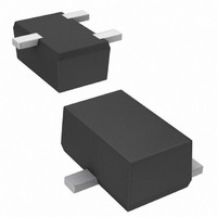
MUN2232T1G ON Semiconductor, MUN2232T1G Datasheet

MUN2232T1G
Specifications of MUN2232T1G
Available stocks
Related parts for MUN2232T1G
MUN2232T1G Summary of contents
Page 1
MUN2211T1 Series Preferred Devices Bias Resistor Transistors NPN Silicon Surface Mount Transistors with Monolithic Bias Resistor Network This new series of digital transistors is designed to replace a single device and its external resistor bias network. The BRT (Bias Resistor ...
Page 2
... MUN2216T1 SC-59 MUN2216T1G SC-59 (Pb-Free) MUN2230T1 SC-59 MUN2230T1G SC-59 (Pb-Free) MUN2231T1 (Note 3) SC-59 MUN2231T1G (Note 3) SC-59 (Pb-Free) MUN2232T1 SC-59 MUN2232T1G SC-59 (Pb-Free) MUN2233T1 SC-59 MUN2233T1G SC-59 (Pb-Free) MUN2234T1 (Note 3) SC-59 MUN2234T1G (Note 3) SC-59 (Pb-Free) MUN2236T1 SC-59 MUN2236T1G SC-59 (Pb-Free) MUN2237T1 ...
Page 3
ELECTRICAL CHARACTERISTICS Characteristic OFF CHARACTERISTICS Collector‐Base Cutoff Current ( Collector‐Emitter Cutoff Current ( Emitter‐Base Cutoff Current ( mA, I Collector‐Base ...
Page 4
ELECTRICAL CHARACTERISTICS Characteristic ON CHARACTERISTICS (Note 5) (Continued) Output Voltage ( 1 1.0 kW ...
Page 5
MUN2211T1 Series 350 300 250 200 150 100 R = 370°C/W 50 qJA AMBIENT TEMPERATURE (°C) A Figure 1. Derating Curve http://onsemi.com 5 100 150 ...
Page 6
TYPICAL ELECTRICAL CHARACTERISTICS - MUN2211T1 0.1 0.01 0.001 COLLECTOR CURRENT (mA) C Figure 2. V versus I CE(sat ...
Page 7
TYPICAL ELECTRICAL CHARACTERISTICS - MUN2212T1 0.1 0.01 0.001 COLLECTOR CURRENT (mA) C Figure 7. V versus I CE(sat ...
Page 8
TYPICAL ELECTRICAL CHARACTERISTICS - MUN2213T1 -25° 25°C 1 0.1 0. COLLECTOR CURRENT (mA) C Figure 12. V versus I CE(sat) 1 0.8 0.6 0.4 0.2 ...
Page 9
TYPICAL ELECTRICAL CHARACTERISTICS - MUN2214T1 0.1 0.01 0.001 COLLECTOR CURRENT (mA) C Figure 17. V versus I CE(sat) 4 3.5 3 2.5 2 1 ...
Page 10
TYPICAL ELECTRICAL CHARACTERISTICS — MUN2215T1 0.1 -25°C 25°C 0.01 0.001 COLLECTOR CURRENT (mA) C Figure 22. V versus I CE(sat) 4.5 4 3.5 3 2.5 2 1.5 ...
Page 11
TYPICAL ELECTRICAL CHARACTERISTICS — MUN2216T1 0.1 -25°C 25°C 0.01 0.001 COLLECTOR CURRENT (mA) C Figure 27. V versus I CE(sat) 4.5 4 3.5 3 2.5 2 1.5 ...
Page 12
TYPICAL ELECTRICAL CHARACTERISTICS — MUN2230T1 0.1 -25°C 25°C 0.01 0.001 COLLECTOR CURRENT (mA) C Figure 32. V versus I CE(sat) 4.5 4 3.5 3 2.5 2 1.5 ...
Page 13
TYPICAL ELECTRICAL CHARACTERISTICS — MUN2232T1 75°C 0.1 -25°C 25°C 0.01 0.001 COLLECTOR CURRENT (mA) C Figure 37. V versus I CE(sat ...
Page 14
TYPICAL ELECTRICAL CHARACTERISTICS — MUN2233T1 0.1 -25°C 25°C 0.01 0.001 COLLECTOR CURRENT (mA) C Figure 42. V versus I CE(sat) 4 3.5 3 2.5 2 1.5 1 ...
Page 15
TYPICAL ELECTRICAL CHARACTERISTICS - MUN2236T1 -25°C A 0.1 0. COLLECTOR CURRENT (mA) C Figure 47. V versus I CE(sat) 5 4.5 4 3.5 ...
Page 16
TYPICAL ELECTRICAL CHARACTERISTICS - MUN2237T1 -25°C A 0.1 0. COLLECTOR CURRENT (mA) C Figure 52. V versus I CE(sat) 2 1.8 1.6 1.4 ...
Page 17
MUN2211T1 Series TYPICAL APPLICATIONS FOR NPN BRTs +12 V FROM mP OR OTHER LOGIC Figure 57. Level Shifter: Connects Volt Circuits to Logic V CC OUT IN Figure 58. Open Collector Inverter: Inverts the Input Signal Figure ...
Page 18
... A A1 *For additional information on our Pb-Free strategy and soldering details, please download the ON Semiconductor Soldering and Mounting Techniques Reference Manual, SOLDERRM/D. ON Semiconductor and are registered trademarks of Semiconductor Components Industries, LLC (SCILLC). SCILLC reserves the right to make changes without further notice to any products herein. SCILLC makes no warranty, representation or guarantee regarding the suitability of its products for any particular purpose, nor does SCILLC assume any liability arising out of the application or use of any product or circuit, and specifically disclaims any and all liability, including without limitation special, consequential or incidental damages. “ ...


