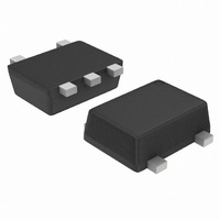
EMC3DXV5T1G ON Semiconductor, EMC3DXV5T1G Datasheet

EMC3DXV5T1G
Specifications of EMC3DXV5T1G
EMC3DXV5T1GOSTR
Available stocks
Related parts for EMC3DXV5T1G
EMC3DXV5T1G Summary of contents
Page 1
... EMC2DXV5T1G, EMC3DXV5T1G, EMC4DXV5T1G, EMC5DXV5T1G Dual Common Base-Collector Bias Resistor Transistors NPN and PNP Silicon Surface Mount Transistors with Monolithic Bias Resistor Network The BRT (Bias Resistor Transistor) contains a single transistor with a monolithic bias network consisting of two resistors; a series base resistor and a base−emitter resistor. These digital transistors are designed to replace a single device and its external resistor bias network ...
Page 2
... FR−4 @ Minimum Pad DEVICE ORDERING INFORMATION, MARKING AND RESISTOR VALUES Transistor 1 − PNP Device Marking R1 (K) EMC2DXV5T1G UC EMC3DXV5T1G U3 EMC3DXV5T5G EMC4DXV5T1G UE EMC5DXV5T1G U5 †For information on tape and reel specifications, including part orientation and tape sizes, please refer to our Tape and Reel Packaging Specifications Brochure, BRD8011/D. *This package is inherently Pb− ...
Page 3
ELECTRICAL CHARACTERISTICS Characteristic Q1 TRANSISTOR: PNP OFF CHARACTERISTICS Collector-Base Cutoff Current ( Collector-Emitter Cutoff Current ( Emitter-Base Cutoff Current ( CHARACTERISTICS ...
Page 4
TYPICAL ELECTRICAL CHARACTERISTICS − EMC2DXV5T1 PNP TRANSISTOR -25°C A 0.1 0. COLLECTOR CURRENT (mA) C Figure 2. V versus I CE(sat ...
Page 5
TYPICAL ELECTRICAL CHARACTERISTICS − EMC2DXV5T1 NPN TRANSISTOR 0.1 0.01 0.001 COLLECTOR CURRENT (mA) C Figure 7. V versus I CE(sat ...
Page 6
TYPICAL ELECTRICAL CHARACTERISTICS − EMC3DXV5T1 PNP TRANSISTOR -25°C A 0.1 75°C 0. COLLECTOR CURRENT (mA) C Figure 12. V versus I CE(sat ...
Page 7
TYPICAL ELECTRICAL CHARACTERISTICS − EMC3DXV5T1 NPN TRANSISTOR -25°C A 0.1 0.01 0.001 COLLECTOR CURRENT (mA) C Figure 17. V versus I CE(sat ...
Page 8
TYPICAL ELECTRICAL CHARACTERISTICS −EMC4DXV5T1 PNP TRANSISTOR 0.1 75°C 0.01 0.001 COLLECTOR CURRENT (mA) C Figure 22. V versus I CE(sat) 4.5 4 3.5 3 2.5 2 1.5 ...
Page 9
TYPICAL ELECTRICAL CHARACTERISTICS − EMC5DXV5T1 PNP TRANSISTOR 0.1 0. COLLECTOR CURRENT (mA) C Figure 28. V versus I CE(sat SERIES 1 ...
Page 10
TYPICAL ELECTRICAL CHARACTERISTICS − EMC4DXV5T1, EMC5DXV5T1 NPN TRANSISTOR -25°C A 0.1 0. COLLECTOR CURRENT (mA) C Figure 32. V versus I CE(sat) 1 0.8 0.6 0.4 ...
Page 11
... Pb−Free strategy and soldering details, please download the ON Semiconductor Soldering and Mounting Techniques Reference Manual, SOLDERRM/D. ON Semiconductor and are registered trademarks of Semiconductor Components Industries, LLC (SCILLC). SCILLC reserves the right to make changes without further notice to any products herein ...


