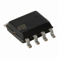
ACS102-5T1-TR STMicroelectronics, ACS102-5T1-TR Datasheet

ACS102-5T1-TR
Specifications of ACS102-5T1-TR
Available stocks
Related parts for ACS102-5T1-TR
ACS102-5T1-TR Summary of contents
Page 1
... Allows straightforward connection of several ACS™ on same cooling pad. DESCRIPTION The ACS102 belongs to the AC line switch family built around the ASD™ concept. This high perfor- mance device is able to control 0.3 A load device. The ACS™ switch embeds a high voltage clamp- ...
Page 2
... ACS102-5Tx ABSOLUTE RATINGS (limiting values) Symbol Repetitive peak off-state voltage DRM RRM I RMS on-state current full cycle sine T(RMS) wave Non repetitive surge peak on-state current TSM Tj initial = 25°C, full cycle sine wave dI/dt Critical rate of repetitive rise of on-state current I = 10mA with tr = 100ns ...
Page 3
... The SO-8 version allows to connect several ACS102 devices on the same cooling PCB pad which is the COM pin. In appliance systems, the ACS102 switch intends to drive low power loads in full cycle ON / OFF mode. The turn off commutation characteristics of these loads are described in Table 1. ...
Page 4
... T AC LINE TRANSIENT VOLTAGE RUGGEDNESS The ACS102 switch is able to withstand safely the AC line transient voltages either by clamping the low en- ergy spikes or by breaking over under high energy shocks. The test circuit of the figure 3 is representative of the final ACS™ application and is also used to stress the ACS™ ...
Page 5
... Fig. 7-2: Relative variation of thermal impedance junction to ambient versus pulse duration (printed circuit board FR4, e(Cu S(Cu) = 40mm under “com” pins) (ACS102-5T1) (SO-8). Zth(j-a) / Rth(j-a) 1.00 0.10 0.01 1E+1 1E+2 5E+2 1E-3 Fig. 9: Relative variation of holding and latching current versus junction temperature. IH,IL [Tj] / IH,IL [Tj=25° ...
Page 6
... One cycle 10.0 1.0 0.1 0.01 100 1000 Fig. 13: Thermal resistance junction to ambient versus copper surface under tab (Epoxy printed circuit board FR4, copper thickness under “com” pins (ACS102-5T1). Rth(j-a) (°C/W) 180 160 140 120 100 max. 40 Vto = 0.85 V ...
Page 7
... V DRM 5 = 500V Gate sensistivity REF 45° 0.25mm A2 (Gage Plane ddd 0.6 1.27 ACS102-5Tx - SO-8 Tape & Reel DIMENSIONS Millimetres Inches Min. Max. Min. Max. 1.35 1.75 0.053 0.069 0.1 0.25 0.004 0.010 1.10 1.65 0.043 0.065 0.33 0.51 0.013 0.020 0.19 ...
Page 8
... ACS102-5TA-TR ACS102 ACS102-5T1 ACS102 ACS102-5T1-TR ACS102 ASD and ACS are a trademarks of STMicroelectronics. Information furnished is believed to be accurate and reliable. However, STMicroelectronics assumes no responsibility for the consequences of use of such information nor for any infringement of patents or other rights of third parties which may result from its use. No license is granted by implication or otherwise under any patent or patent rights of STMicroelectronics ...


