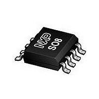
TJA1050T/V.112 NXP Semiconductors, TJA1050T/V.112 Datasheet - Page 3

TJA1050T/V.112
Manufacturer Part Number
TJA1050T/V.112
Description
Manufacturer
NXP Semiconductors
Datasheet
1.TJA1050TV.112.pdf
(18 pages)
Specifications of TJA1050T/V.112
Number Of Transceivers
1
Power Down Mode
Standby
Standard Supported
ISO 11898
Operating Supply Voltage (max)
5.25V
Operating Supply Voltage (typ)
5V
Operating Supply Voltage (min)
4.75V
Package Type
SO
Supply Current
10mA
Operating Temperature (max)
150C
Operating Temperature (min)
-40C
Operating Temperature Classification
Automotive
Mounting
Surface Mount
Pin Count
8
Lead Free Status / RoHS Status
Compliant
Philips Semiconductors
BLOCK DIAGRAM
PINNING
2003 Oct 22
handbook, full pagewidth
TXD
GND
V
RXD
V
CANL
CANH
S
SYMBOL
CC
ref
High speed CAN transceiver
PIN
RXD
TXD
V ref
1
2
3
4
5
6
7
8
S
transmit data input; reads in data
from the CAN controller to the bus
line drivers
ground
supply voltage
receive data output; reads out
data from the bus lines to the
CAN controller
reference voltage output
LOW-level CAN bus line
HIGH-level CAN bus line
select input for high-speed mode
or silent mode
8
1
4
5
200
A
V CC
GND
V CC
DESCRIPTION
GND
REFERENCE
DOMINANT
TIME-OUT
VOLTAGE
TIMER
30 A
TXD
Fig.1 Block diagram.
RECEIVER
TEMPERATURE
PROTECTION
TJA1050
3
handbook, halfpage
DRIVER
GND
V CC
RXD
TXD
0.5V CC
Fig.2 Pin configuration.
GND
V CC
1
2
3
4
GND
2
3
TJA1050T
MGS374
k
k
MGS375
25
25
7
6
7
6
5
8
Product specification
CANH
CANL
S
CANL
V ref
CANH
TJA1050


