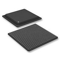
XC6SLX150-2FGG484C Xilinx Inc, XC6SLX150-2FGG484C Datasheet - Page 62

XC6SLX150-2FGG484C
Manufacturer Part Number
XC6SLX150-2FGG484C
Description
FPGA, SPARTAN-6 LX, 147K, 484FGGBGA
Manufacturer
Xilinx Inc
Series
Spartan® 6 LXr
Datasheet
1.XC6SLX45-2FGG484CES.pdf
(76 pages)
Specifications of XC6SLX150-2FGG484C
No. Of Logic Blocks
23038
No. Of Macrocells
147443
Family Type
Spartan-6
No. Of Speed Grades
2
Total Ram Bits
4939776
No. Of I/o's
338
Clock Management
DCM, PLL
I/o Supply Voltage
3.3V
Package / Case
484-BGA
Mounting Type
Surface Mount
Voltage - Supply
1 V ~ 3.6 V
Operating Temperature
0°C ~ 85°C
Number Of I /o
338
Number Of Logic Elements/cells
147443
Rohs Compliant
Yes
Lead Free Status / RoHS Status
Lead free / RoHS Compliant
Number Of Gates
-
Lead Free Status / RoHS Status
Lead free / RoHS Compliant, Lead free / RoHS Compliant
Available stocks
Company
Part Number
Manufacturer
Quantity
Price
Company:
Part Number:
XC6SLX150-2FGG484C
Manufacturer:
XILINX
Quantity:
1 043
Company:
Part Number:
XC6SLX150-2FGG484C
Manufacturer:
Xilinx Inc
Quantity:
10 000
Spartan-6 Device Pin-to-Pin Input Parameter Guidelines
All devices are 100% functionally tested. The representative values for typical pin locations and normal clock loading are
listed in
Table 68: Global Clock Setup and Hold Without DCM or PLL
DS162 (v2.0) March 31, 2011
Preliminary Product Specification
Notes:
1.
2.
Input Setup and Hold Time Relative to Global Clock Input Signal for LVCMOS25 Standard.
T
PSFD
Setup and Hold times are measured over worst case conditions (process, voltage, temperature). Setup time is measured relative to the Global Clock
input signal using the slowest process, highest temperature, and lowest voltage. Hold time is measured relative to the Global Clock input signal using
the fastest process, lowest temperature, and highest voltage.
IFF = Input Flip-Flop or Latch.
Symbol
/ T
Table 68
PHFD
through
No Delay Global Clock and IFF
or PLL
Table
74. Values are expressed in nanoseconds unless otherwise noted.
Description
(2)
without DCM
www.xilinx.com
Spartan-6 FPGA Data Sheet: DC and Switching Characteristics
XC6SLX4
XC6SLX9
XC6SLX16
XC6SLX25
XC6SLX25T
XC6SLX45
XC6SLX45T
XC6SLX75
XC6SLX75T
XC6SLX100
XC6SLX100T
XC6SLX150
XC6SLX150T
Device
–0.08/
–0.08/
–0.14/
–0.14/
–0.24/
–0.24/
0.10/
0.10/
0.12/
0.18/
0.18/
0.13/
0.13/
1.56
1.56
1.42
1.64
1.64
1.80
1.88
1.97
1.81
2.15
2.03
2.42
2.55
-3
(1)
–0.08/
–0.08/
–0.14/
–0.14/
–0.24/
–0.24/
0.10/
0.12/
0.18/
0.18/
0.13/
0.13/
1.57
1.48
1.75
1.75
1.95
1.95
2.06
2.06
2.24
2.24
2.74
2.74
Speed Grade
-3N
N/A
–0.08/
–0.08/
–0.14/
–0.14/
–0.24/
–0.24/
0.10/
0.10/
0.12/
0.18/
0.18/
0.13/
0.13/
1.83
1.84
1.64
1.99
1.99
2.27
2.27
2.27
2.27
2.56
2.56
2.95
2.95
-2
–0.17/
–0.12/
–0.17/
–0.60/
0.07/
0.07/
0.13/
0.11/
2.54
2.54
2.19
2.57
2.74
3.20
3.44
3.75
N/A
N/A
N/A
N/A
N/A
-1L
Units
ns
ns
ns
ns
ns
ns
ns
ns
ns
ns
ns
ns
ns
62


