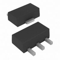
MCP1701AT-4602I/MB Microchip Technology, MCP1701AT-4602I/MB Datasheet - Page 11

MCP1701AT-4602I/MB
Manufacturer Part Number
MCP1701AT-4602I/MB
Description
Low Iq 250mA LDO, Vin 10V Max, Vout=4.6V 3 SOT-89 T/R
Manufacturer
Microchip Technology
Specifications of MCP1701AT-4602I/MB
Regulator Topology
Positive Fixed
Voltage - Output
4.6V
Voltage - Input
Up to 10V
Number Of Regulators
1
Operating Temperature
-40°C ~ 85°C
Mounting Type
Surface Mount
Package / Case
SC-62, SOT-89, TO-243 (3 Leads + Tab)
Number Of Outputs
1
Polarity
Positive
Input Voltage Max
10 V
Output Voltage
4.6 V
Output Type
Fixed
Voltage Regulation Accuracy
2 %
Maximum Operating Temperature
+ 85 C
Mounting Style
SMD/SMT
Minimum Operating Temperature
- 40 C
Lead Free Status / RoHS Status
Lead free / RoHS Compliant
Current - Output
-
Voltage - Dropout (typical)
-
Current - Limit (min)
-
Lead Free Status / Rohs Status
Lead free / RoHS Compliant
Available stocks
Company
Part Number
Manufacturer
Quantity
Price
Part Number:
MCP1701AT-4602I/MB
Manufacturer:
MICROCHIP/微芯
Quantity:
20 000
5.0
5.1
The amount of power dissipated internal to the LDO
linear regulator is the sum of the power dissipation
within the linear pass device (P-channel MOSFET) and
the quiescent current required to bias the internal
reference and error amplifier. The internal linear pass
device power dissipation is calculated as shown in
Equation 5-1.
EQUATION 5-1:
The internal power dissipation, as a result of the bias
current for the LDO internal reference and error
amplifier, is calculated as shown in Equation 5-2.
EQUATION 5-2:
The total internal power dissipation is the sum of P
(pass device) and P
EQUATION 5-3:
For the MCP1701, the internal quiescent bias current is
so low (2 µA, typ.) that the P
dissipation equation can be ignored. The maximum
power dissipation can be estimated by using the
maximum input voltage and the minimum output
voltage to obtain a maximum voltage differential
between input and output. The next step would be to
multiply the maximum voltage differential by the
maximum output current.
EQUATION 5-4:
© 2005 Microchip Technology Inc.
Given:
T
P
P
V
AMAX
I
MAX
MAX
OUT
OUT
V
IN
P
TOTAL
THERMAL CONSIDERATIONS
Power Dissipation
P
P
D
= 3.3V to 4.1V
= 3.0V ± 2%
= 1 mA to 100 mA
= 55°C
= (4.1V – (3.0V x 0.98)) x 100 mA
= 116.0 milliwatts
D
(Pass Device) = (V
= (V
= P
P
INMAX
D
D
(Pass Device) + P
(Bias) = V
D
(bias).
– V
OUTMIN
D
IN
IN
(bias) term of the power
– V
x I
) x I
GND
OUT
D
OUTMAX
(Bias)
) x I
OUT
D
To determine the junction temperature of the device, the
thermal resistance from junction-to-ambient must be
known. The 3-pin SOT-23 thermal resistance from
junction-to-air (R
335° C/W. The SOT-89 R
approximately 52° C/W when mounted on 1 square inch
of copper. The R
and other application-specific conditions.
The device junction temperature is determined by
calculating the junction temperature rise above
ambient, then adding the rise to the ambient
temperature.
EQUATION 5-5:
EQUATION 5-6:
T
T
T
T
T
J
J
J
J
J
=
=
=
=
=
P
116.0 milliwatts 335°C/W
93.9°C
116.0 milliwatts 52°C/W
61°C
DMAX
JA
JA
will vary with physical layout, airflow
) is estimated to be approximately
JUNCTION
TEMPERATURE – SOT-23
EXAMPLE:
JUNCTION
TEMPERATURE – SOT-89
EXAMPLE:
R
JA
+
MCP1701
T
JA
A
is estimated to be
DS21874B-page 11
+
+
55°C
55°C


