MCP635T-E/UN Microchip Technology, MCP635T-E/UN Datasheet - Page 19
MCP635T-E/UN
Manufacturer Part Number
MCP635T-E/UN
Description
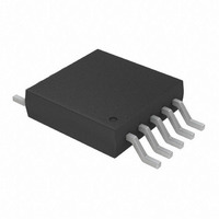
Dual, 24MHz OP W /CS, E Temp 10 MSOP 3x3mm T/R
Manufacturer
Microchip Technology
Datasheet
1.MCP631-ESN.pdf
(42 pages)
Specifications of MCP635T-E/UN
Amplifier Type
General Purpose
Number Of Circuits
2
Output Type
Rail-to-Rail
Slew Rate
10 V/µs
Gain Bandwidth Product
24MHz
Current - Input Bias
4pA
Voltage - Input Offset
1800µV
Current - Supply
2.5mA
Current - Output / Channel
70mA
Voltage - Supply, Single/dual (±)
2.5 V ~ 5.5 V
Operating Temperature
-40°C ~ 125°C
Mounting Type
Surface Mount
Package / Case
10-MSOP, Micro10™, 10-uMAX, 10-uSOP
Number Of Channels
2
Voltage Gain Db
124 dB
Common Mode Rejection Ratio (min)
63 dB
Input Offset Voltage
8 mV
Operating Supply Voltage
3 V, 5 V
Maximum Operating Temperature
+ 125 C
Mounting Style
SMD/SMT
Minimum Operating Temperature
- 40 C
Lead Free Status / RoHS Status
Lead free / RoHS Compliant
-3db Bandwidth
-
Lead Free Status / Rohs Status
Details
Available stocks
Company
Part Number
Manufacturer
Quantity
Price
Company:

Part Number:
MCP635T-E/UN
Manufacturer:
MICROCHIP
Quantity:
12 000


3.0
Descriptions of the pins are listed in
TABLE 3-1:
3.1
The analog output pins (V
voltage sources.
3.2
The non-inverting and inverting inputs (V
are high-impedance CMOS inputs with low bias
currents.
3.3
The positive power supply (V
than the negative power supply (V
operation, the other pins are between V
Typically, these parts are used in a single (positive)
supply configuration. In this case, V
ground and V
need bypass capacitors.
© 2009 Microchip Technology Inc.
MCP631
SOIC
1,5,8
—
—
—
—
—
—
6
2
3
4
7
PIN DESCRIPTIONS
Analog Outputs
Analog Inputs
Power Supply Pins
SOIC
DD
—
—
—
—
MCP632
1
2
3
4
5
6
7
8
is connected to the supply. V
PIN FUNCTION TABLE
DFN
—
—
—
1
2
3
4
5
6
7
8
9
OUT
DD
MCP633
SOIC
) is 2.5V to 5.5V higher
1,5
—
—
—
—
—
) are low-impedance
6
2
3
4
8
7
SS
Table
SS
is connected to
SS
). For normal
IN
MSOP
3-1.
and V
+, V
10
—
—
MCP635
1
2
3
4
5
6
7
8
9
IN
DD
DD
–, …)
DFN
.
will
10
11
—
1
2
3
4
5
6
7
8
9
V
V
V
OUT
IN
CS, CS
IN
Symbol
V
V
V
+, V
–, V
CS
V
V
3.4
This input (CS) is a CMOS, Schmitt-triggered input that
places the part into a low power mode of operation.
3.5
There is an internal connection between the Exposed
Thermal Pad (EP) and the V
connected to the same potential on the Printed Circuit
Board (PCB).
This pad can be connected to a PCB ground plane to
provide a larger heat sink. This improves the package
thermal resistance (θ
OUTB
NC
EP
INB
INB
, V
DD
SS
B
OUTA
INA
INA
+
–
A
–
+
Chip Select Digital Input (CS)
Exposed Thermal Pad (EP)
Output (op amp A)
Inverting Input (op amp A)
Non-inverting Input (op amp A)
Negative Power Supply
Chip Select Digital Input (op amp A)
Chip Select Digital Input (op amp B)
Non-inverting Input (op amp B)
Inverting Input (op amp B)
Output (op amp B)
Positive Power Supply
No Internal Connection
Exposed Thermal Pad (EP);
must be connected to V
MCP631/2/3/5
JA
).
Description
SS
SS
pin; they must be
DS22197A-page 19
Related parts for MCP635T-E/UN
Image
Part Number
Description
Manufacturer
Datasheet
Request
R

Part Number:
Description:
Dual, 24MHz OP W /CS, E Temp 10 DFN 3x3mm T/R
Manufacturer:
Microchip Technology
Datasheet:

Part Number:
Description:
Manufacturer:
Microchip Technology Inc.
Datasheet:
Part Number:
Description:
Manufacturer:
Microchip Technology Inc.
Datasheet:
Part Number:
Description:
Manufacturer:
Microchip Technology Inc.
Datasheet:
Part Number:
Description:
Manufacturer:
Microchip Technology Inc.
Datasheet:
Part Number:
Description:
Manufacturer:
Microchip Technology Inc.
Datasheet:
Part Number:
Description:
Manufacturer:
Microchip Technology Inc.
Datasheet:
Part Number:
Description:
Manufacturer:
Microchip Technology Inc.
Datasheet:
Part Number:
Description:
Manufacturer:
Microchip Technology Inc.
Datasheet: