MCP98242T-BE/MNY Microchip Technology, MCP98242T-BE/MNY Datasheet - Page 33

MCP98242T-BE/MNY
Manufacturer Part Number
MCP98242T-BE/MNY
Description
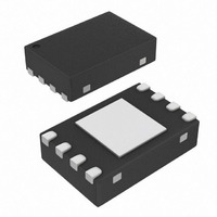
IC,TEMPERATURE SENSOR,LLCC,8PIN,PLASTIC
Manufacturer
Microchip Technology
Datasheets
1.MCP98242T-CEMC.pdf
(56 pages)
2.MCP98242T-CEMC.pdf
(6 pages)
3.MCP98242T-BEMUY.pdf
(48 pages)
Specifications of MCP98242T-BE/MNY
Function
Temp Monitoring System (Sensor)
Topology
ADC (Sigma Delta), Register Bank
Sensor Type
Internal
Sensing Temperature
-40°C ~ 125°C
Output Type
I²C™/SMBus™
Output Alarm
Yes
Output Fan
Yes
Voltage - Supply
3 V ~ 3.6 V
Operating Temperature
-40°C ~ 125°C
Mounting Type
Surface Mount
Package / Case
8-DFN
Full Temp Accuracy
+/- 2 C
Digital Output - Bus Interface
Serial (2-Wire, I2C)
Maximum Operating Temperature
+ 125 C
Minimum Operating Temperature
- 40 C
Lead Free Status / RoHS Status
Lead free / RoHS Compliant
Lead Free Status / RoHS Status
Lead free / RoHS Compliant
Other names
MCP98242T-BE/MNY
MCP98242T-BE/MNYTR
MCP98242T-BE/MNYTR
Available stocks
Company
Part Number
Manufacturer
Quantity
Price
Company:
Part Number:
MCP98242T-BE/MNY
Manufacturer:
MICROCHIP
Quantity:
12 000
5.3.3.1
The SWP feature is invoked by writing to the
write-protect register. This is done by sending an
Address Byte similar to a normal Write command.
Figure 5-14
cleared
Section 5.3.3.2 “Clear Write-Protect
FIGURE 5-12:
Communication”).
5.3.3.2
The CWP feature is invoked by writing to the clear
write-protect register. This is done by sending an
Address Byte similar to a normal Write command.
Figure 5-14
SWP only. PWP can not be cleared using this
command.
FIGURE 5-13:
Communication”).
2010 Microchip Technology Inc.
SCLK
SCLK
SDA
SDA
Note:
Note:
using
shows the timing diagram. SWP can be
shows the timing diagram. CWP clears
Software Write-Protect (SWP)
Clear Write-Protect (CWP)
S
S
Apply V
1
Apply V
1
0
0
the
2
1
Timing Diagram for Setting Software Write-Protect (See
2
1
Timing Diagram for Setting Clear Write-Protect (See
Address Byte
Address Byte
3
1
3
1
HI_WP
CWP
HI_WP
4
4
0
0
5
5
0
0
at A0 pin, apply V
at A0 pin and connect GND to A1 and A2 pins to initiate SWP cycle.
6
6
0
1
command.
(CWP)”.
7
7
1
1
MCP98242
MCP98242
W
W
8
8
A
C
K
A
C
K
1
1
X
X
See
DD
2
2
X
X
Word Address
Word Address
at A1 pin, connect A2 pin to GND to initiate CWP cycle.
3
3
X
X
4
4
X
X
5
5
X
X
The Slave Address bits need to correspond to the
address pin logic configuration. For SWP, a high
voltage V
the corresponding slave address needs to be set to ‘1’,
as shown in
grounded and the corresponding slave address bits are
set to ‘0’.
The device response in this mode is shown in
Table 5-4
The Slave Address bits need to correspond to the
address pin logic configuration. For CWP, a high
voltage V
the corresponding slave address needs to be set to ‘1’.
The A1 pin is set to V
address bit is set to ‘1’. And A2 pin is set to ground
and the corresponding slave address bits are set to ‘0’.
Table 5-3
response in this mode is shown in
Table
6
X
6
X
7
7
X
X
5-5.
MCP98242
MCP98242
8
8
X
X
HI_WP
HI_WP
and
shows the bit configuration. The device
A
C
K
A
C
K
Table
Table
1
1
X
X
needs to be applied to the A0 pin and
needs to be applied to the A0 pin and
Section 4.0 “Serial
2
2
X
X
5-3. Both A2 and A1 pins are
5-5.
3
3
Section 4.0 “Serial
X
X
DD
Data
Data
4
4
X
X
and the corresponding slave
MCP98242
5
5
X
X
6
X
6
X
7
7
X
X
MCP98242
MCP98242
DS21996D-page 33
8
8
X
X
Table 5-4
A
C
K
A
C
K
P
P
and


