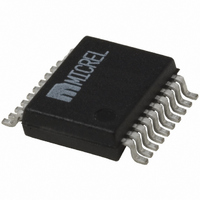
MIC2179-3.3YSM Micrel Inc, MIC2179-3.3YSM Datasheet - Page 8

MIC2179-3.3YSM
Manufacturer Part Number
MIC2179-3.3YSM
Description
IC,SMPS CONTROLLER,CURRENT-MODE,SSOP,20PIN,PLASTIC
Manufacturer
Micrel Inc
Type
Step-Down (Buck)r
Datasheet
1.MIC2179YSM_TR.pdf
(13 pages)
Specifications of MIC2179-3.3YSM
Lead Free Status
Lead free
Internal Switch(s)
Yes
Synchronous Rectifier
Yes
Number Of Outputs
1
Voltage - Output
3.3V
Current - Output
1.5A
Frequency - Switching
200kHz
Voltage - Input
4.5 ~ 16.5 V
Operating Temperature
-40°C ~ 85°C
Mounting Type
Surface Mount
Package / Case
20-SSOP
Power - Output
-
Lead Free Status / RoHS Status
Other names
576-1711-5
MIC2179-3.3YSM
MIC2179-3.3YSM
Available stocks
Company
Part Number
Manufacturer
Quantity
Price
Company:
Part Number:
MIC2179-3.3YSM
Manufacturer:
MIC
Quantity:
16
(V
amplifier output voltage increases. This voltage then intersects
the current sense waveform later in switching period which
increases the duty cycle and the average inductor current. If
V
decreases, reducing the duty cycle.
The PWM control loop is stabilized in two ways. First, the
inner signal loop is compensated by adding a corrective ramp
to the output of the current sense amplifier. This allows the
regulator to remain stable when operating at greater than
50% duty cycle. Second, a series resistor-capacitor load
is connected to the error amplifier output (COMP pin). This
places a pole-zero pair in the regulator control loop.
One more important item is synchronous rectification. As
mentioned earlier, the N-channel output MOSFET is turned
on after the P-channel turns off. When the N-channel turns
on, its on-resistance is low enough to create a short across
the output diode. As a result, inductor current flows through
the N-channel and the voltage drop across it is significantly
lower than a diode forward voltage. This reduces power dis-
sipation and improves efficiency to greater than 95% under
certain operating conditions.
To prevent shoot through current, the output stage employs
break-before-make circuitry that provides approximately 50ns
of delay from the time one MOSFET turns off and the other
turns on. As a result, inductor current briefly flows through
the output diode during this transition.
Skip-Mode Operation
Refer to “Skip Mode Functional Diagram” which is a simplified
block diagram of the MIC2179 operating in skip mode and
its associated waveforms.
Skip-mode operation turns on the output P-channel at a
frequency and duty cycle that is a function of V
the output inductor value. While in skip mode, the N-chan-
nel is kept off to optimize efficiency by reducing gate charge
dissipation. V
that turn on the P-channel.
To begin analyzing MIC2179 skip mode operation, assume
the skip-mode comparator output is high and the latch out-
put has been reset to a logic 1. This turns on the P-channel
and causes I
limit of 400mA. When I
comparator sets the RS latch output to logic 0, turning off
June 2009
OUT
REF
is higher than nominal, the error amplifier output voltage
). When V
L1
OUT
to increase linearly until it reaches a current
OUT
is regulated by skipping switching cycles
is lower than its nominal value, the error
L1
reaches this value, the current limit
IN
, V
OUT
, and
8
the P-channel. The output switch voltage (V
from V
Schottky diode. L1 discharges its energy to the output and
I
to V
Resetting the RS latch turns on the P-channel, and this begins
another switching cycle.
The skip-mode comparator regulates V
when the MIC2179 skips cycles. It compares V
and has 10mV of hysteresis to prevent oscillations in the
control loop. When V
parator output is logic 1, allowing the P-channel to turn on.
Conversely, when V
channel is turned off.
Note that this is a self oscillating topology which explains
why the switching frequency and duty cycle are a function
of V
(for a pulse-skipping regulator) of supplying the same value
of maximum load current for any value of V
This allows the MIC2179 to always supply up to 300mA of
load current when operating in skip mode.
Selecting PWM- or Skip-Mode Operation
PWM or skip mode operation is selected by an external
logic signal applied to the PWM pin. A logic low places the
MIC2179 into PWM mode, and logic high places it into skip
mode. Skip mode operation provides the best efficiency when
load current is less than 150mA, and PWM operation is more
efficient at higher currents.
The MIC2179 was designed to be used in intelligent sys-
tems that determine when it should operate in PWM or skip
mode. This makes the MIC2179 ideal for applications where
a regulator must guarantee low noise operation when sup-
plying light load currents, such as cellular telephone, audio,
and multimedia circuits.
There are two important items to be aware of when selecting
PWM or skip mode. First, the MIC2179 can start-up only in
PWM mode, and therefore requires a logic low at PWM dur-
ing start-up. Second, in skip mode, the MIC2179 will supply
a maximum load current of approximately 300mA, so the
output will drop out of regulation when load current exceeds
this limit. To prevent this from occurring, the MIC2179 should
change from skip to PWM mode when load current exceeds
200mA.
L1
decreases to zero. When I
OUT
IN
, V
IN
, and this triggers a one-shot that resets the RS latch.
OUT
to 0.4V below ground, and I
, and the value of L1. It has the unique feature
FB
FB
is greater than V
is less than V
L1
= 0, V
SW
REF
L1
REF
OUT
swings from –0.4V
flows through the
– 5mV, the com-
SW
IN
+ 5mV, the P-
by controlling
, V
M9999-063009
) then swings
FB
OUT
to V
, or L1.
REF


