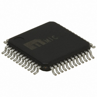
MIC2341R-2YTQ Micrel Inc, MIC2341R-2YTQ Datasheet - Page 18

MIC2341R-2YTQ
Manufacturer Part Number
MIC2341R-2YTQ
Description
Dual -Slot PCI Express Hot-Plug Controller
Manufacturer
Micrel Inc
Type
Hot-Swap Controllerr
Datasheet
1.MIC2341R-2YTQ.pdf
(32 pages)
Specifications of MIC2341R-2YTQ
Applications
General Purpose, PCI Express
Internal Switch(s)
No
Current Limit
Adjustable
Voltage - Supply
3.3V, 12V
Operating Temperature
0°C ~ 70°C
Mounting Type
Surface Mount
Package / Case
48-TQFP
Lead Free Status / RoHS Status
Lead free / RoHS Compliant
Other names
576-2987
Available stocks
Company
Part Number
Manufacturer
Quantity
Price
Functional Description
Hot Swap Insertion
When circuit boards are inserted into systems carrying
live supply voltages (“hot-plugged”), high inrush currents
often result due to the charging of bulk capacitance that
resides across the circuit board’s supply pins. This
transient inrush current can cause the system’s supply
voltages to temporarily go out of regulation, causing data
loss or system lock-up. In more extreme cases, the
transients occurring during a hot-plug event may cause
permanent
components.
The MIC2341 addresses these issues by limiting the
inrush currents to the load (PCI Express Board), and
thereby controlling the rate at which the load’s circuits
turn-on. In addition to this inrush current control, the
MIC2341 offers input and output voltage supervisory
functions and current limiting to provide robust protection
for both the system and circuit board.
System Interface
The MIC2341 employs a hardware system interface that
includes:
/FAULT_MAIN[A/B], /FAULT_AUX[A/B], /PWRGD[A/B],
/INT, and SYSPWRGD.
Power-On Reset
VSTBY[A/B] are
MIC2341’s internal logic circuits and state machines .
VSTBY[A/B] is required for proper operation of the
MIC2341’s internal logic circuitry and must be applied at
all times. A Power-On Reset (POR) cycle is initiated
after VSTBY[A/B] is higher than its V
voltage and remains valid at that voltage for at least
80µs. All internal logic flags are cleared after POR. If the
VSTBY[A/B] pin voltages are cycled ON-OFF-ON, a
new power-on-reset cycle is initiated. V
first supply input applied followed by the MAIN supply
inputs of 12V
off. In most applications, the total POR interval will
consist of the time required to charge the V
(bypass) capacitance to the UVLO threshold plus the
internal t
to approximate the total POR interval:
where C
and I
source to charge the capacitance.
Micrel, Inc.
October 2007
t
POR_TOTAL(
CHARGE(STBY)
STBY
POR
µs)
ON[A/B],
delay time. The following equation is used
is the V
damage
IN
=
and 3V
⎧
⎪
⎨
⎪ ⎩
⎡
⎢
⎢
⎣
is the current supplied by the V
(
C
STBY(µF)
the main power supply for the
STBY
I
CHARGE(STB
IN
to
. During t
input bulk bypass capacitance
AUXEN[A/B],
×
V
ULVO(STBY)
connectors
Y)
(A)
POR
, all outputs remain
UVLO(STBY)
)
⎤
⎥
⎥
⎦
×
STBY
10
−
or
6
/CRSW[A/B],
⎫
⎪
⎬
⎪ ⎭
must be the
+
STBY
t
threshold
POR
on-board
(µs)
input
STBY
18
+12VOUT[A/B] and +3VOUT[A/B] Start-Up Cycles
All four of the MIC2341’s +12V and +3V gate drive
circuits have been designed to drive the gates of
external power MOSFETs. The +12V gate drive circuits
have been designed to drive P-channel MOSFETs and
the +3V gate drive circuits are intended to drive N-
channel MOSFETs. A list of recommended N- and P-
channel power MOSFETs suited for use with the
MIC2341 and PCI Express applications can be found in
Table 2.
These gate drive circuits have also been designed to
limit inrush current in one of two modes: (1) by
controlling the 12VGATE[A/B] or the 3VGATE[A/B]
voltage slew rates (dV
by actively limiting the inrush current, thereby charging
the corresponding load capacitance in current limit. The
mode that the MIC2341 automatically enters
dependent upon the magnitude of the inrush current and
the magnitude of the load capacitance at 12VOUT[A/B]
and 3VOUT[A/B].
Mode 1: [12V/3V]GATE[A/B] Slew Rate Control
When a slot’s MAIN supply voltages (12VOUT[A/B] and
3VOUT[A/B]) are OFF, each of the 12VGATE[A/B] pins
is held at 12VIN[A/B] by an internal pull-up transistor.
Similarly, each 3VGATE[A/B] pin is internally held at
AGND. When the MAIN supply voltages are enabled by
a low-to-high transition on the ON[A/B] input pins (recall
that the /CRSW[A/B] inputs must also be asserted), the
12VGATE[A/B] and the 3VGATE[A/B] pins are each
connected to an internal constant current supply,
typically 25 µA each. At each 12VGATE[A/B] pin, this
constant current supply is a current sink; at each
3VGATE[A/B] pin, the supply is a current source. For
applications where the inrush current is controlled by the
12VGATE[A/B] voltage rate of change, an expression
for the circuit’s behavior is given by the following
equation:
where C
capacitance.
For example, a Si4435BDY (a 30-V P-channel power
MOSFET) exhibits an approximate C
V
change (slew rate) would be:
The 12VOUT[A/B] inrush current to the load while the
12VGATE[A/B] voltage is ramping is dependent on
C
12VOUT[A/B] inrush current is given by:
DS
LOAD(12VOUT[A/B])
= 12V. The 12VGATE[A/B] pin voltage rate-of-
dV
12VGATE[A/
ISSP
dt
dV
12VGATE[A/
= P-channel power MOSFET gate input
B]
dt
and C
=
I
GATE(12VSN
B]
12GATE[A/B]
C
=
ISSP
ISSP
I
GATE(12VGA
. An expression for the
K)
C
ISSP
/dt or dV
=
1700pF
25µA
TE)
ISSP
=
MIC2341/2341R
3GATE[A/B]
M9999-102507-A
=
C
25µA
14.7
(408) 944-0800
ISSP
of 1700pF at
ms
V
/dt) or (2)
is


