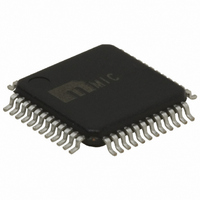
MIC2342R-2YTQ Micrel Inc, MIC2342R-2YTQ Datasheet - Page 19

MIC2342R-2YTQ
Manufacturer Part Number
MIC2342R-2YTQ
Description
Dual -Slot PCI Express Hot-Plug Controller
Manufacturer
Micrel Inc
Type
Hot-Swap Controllerr
Datasheet
1.MIC2342-2YTQ.pdf
(32 pages)
Specifications of MIC2342R-2YTQ
Applications
General Purpose, PCI Express
Internal Switch(s)
No
Current Limit
Adjustable
Voltage - Supply
3.3V, 12V
Operating Temperature
0°C ~ 70°C
Mounting Type
Surface Mount
Package / Case
48-TQFP
Lead Free Status / RoHS Status
Lead free / RoHS Compliant
Other names
576-2996
Available stocks
Company
Part Number
Manufacturer
Quantity
Price
For the same p-channel power MOSFET in the previous
example, if C
100µF, the 12VOUT[A/B] inrush current charging this
load capacitance is:
Calculating the 12VOUT[A/B] voltage rate-of-change for
a given capacitive load can be determined by the
following expression:
and, using the same quantities in the current example, is
given by:
To determine (to first-order) the time point at which the
12VOUT[A/B] voltage crosses its corresponding output
“Power Good” threshold, the following equation can be
used:
To determine 3VGATE[A/B] pin voltage slew rates,
inrush currents, 3VOUT[A/B] output voltage slew rates,
and time to assert its corresponding internal “Power
Good”
3VOUT[A/B], simple computations can be made using
the same equations by substituting I
I
channel power MOSFET) for C
C
and V
For example, if a Si4420BDY n-channel power MOSFET
is used with the MIC2342 to control inrush currents at
3VOUT[A/B], its C
3V. The 3VGATE[A/B] pin voltage rate of change is
given by:
Assuming a 300-µF capacitive load, the 3VOUT[A/B]
inrush current charging this load capacitance is given by:
The 3VOUT[A/B] output voltage slew rate is given by:
and the time to assert the internal 3VOUT[A/B] “Power
Good” flag is given by:
I
=
GATE(12VSINK)
INRUSH(12V
t
Micrel, Inc.
June 2008
LOAD(12VOUT[A/B])
I
PWRGD
GATE(12VSN
UVTH(3V)
dV
(
12
flag
3VGATE[A/B
OUT[A/B])
VOUT
I
I
INRUSH(3VO
INRUSH
K)
, C
dt
dV
ISSP
dV
for V
×
[
A
ISSN
C
12
into
/
12VOUT[A/B
, I
(
B
dV
12
LOAD(12VOU
VOUT
=
])
= 1700pF and C
VOUT
]
dt
3VOUT[A/B]
UVTH(12V)
dt
ISSN
dV
=
INRUSH(3VOUT[A/B])
=
(the input gate capacitance of an N-
UT[A/B])
dt
C
(
V
I
12VGATE[A/
[
[
GATE(3VCHA
A
capacitive
ISSP
A
UVTH
/
/
is approximately 4100pF at V
B
B
dV
dt
]
])
]
C
=
T[A/B])
12
.
=
=
(
=
12
ISSN
=
I
VOUT
25
25
C
INRUSH
V
100
1.47
300
1.82
dt
LOAD
)
B]
µ
µA
+
A
RGE)
×
V
[
µ
×
×
µ
A
A
A
HYSPG
C
F
(
F
/
1700
(
12
4100pF
ISSP
LOAD(12VOUT[A/B])
100
B
12
300
LOAD(12VOU
loads
≈
]
VOUT
=
=
VOUT
for I
6.1
14.7
, C
µF
4100pF
µ
pF
25
F
)
ms
[
=
V
[
A
µ
GATE(3VCHARGE)
A
LOAD(3VOUT[A/B])
=
=
/
A
14
INRUSH(12VOUT[A/B])
ms
/
10
B
1.82
. 1
B
V
connected
])
])
7 .
47
T[A/B])
.
=
53
ms
A
V
6.1
A
V
=
ms
≈
V
. 0
72
DS
ms
for
for
to
=
,
19
Mode 2: Charging 12VOUT and 3VOUT Capacitive
Loads in Current Limit
In x4 and x8 PCI Express applications, capacitive loads
at 12VOUT[A/B] and 3VOUT[A/B] can be as large as
1000µF. As a result, the inrush load charging currents at
start-up can be large enough to cause a voltage drop
across the external sense resistor larger than 50mV. In
these
12VGATE[A/B] and 3VGATE[A/B] modulate the drive to
the gates of their corresponding power MOSFETs to
regulate the load current to:
In the typical application circuit, the external sense
resistor
12VSENSE[A/B] pins was selected to be 20mΩ. The
regulated current charging the load capacitance at
12VOUT[A/B] is given by:
Once current-regulation control is activated, the circuit
breaker’s t
external power MOSFET against potentially excessive
power dissipation. For additional information on this
timer and the MIC2342’s circuit breaker operation,
please consult the section labeled “Circuit Breaker
Function.” The output voltage rate of change at
12VOUT[A/B] during current limit charging into a 1000µF
capacitive load is given by:
In this fashion, the inrush current is controlled and the
load capacitance is charged up slowly during the start-up
cycle. The gate drive circuits will maintain control of the
inrush current until the 12VOUT[A/B] or 3VOUT[A/B]
voltages have reached their corresponding “Power
Good”
respectively)
approaches its nominal steady-state level, the voltage
across the external sense resistor drops below the circuit
breaker’s V
internal “Power-is-Good” flag is asserted. For the
12VOUT[A/B] example, its internal “Power-is-Good” flag
is asserted at:
Calculating the current limit for charging the 3VOUT[A/B]
load capacitance, the output voltage slew rate at
t
t
PWRGD(12VO
PWRGD(3VOU
dV
I
LIMIT(12VO
12VOUT[A/B
applications,
thresholds
dt
connected
FLT
THLIMIT
UT[A/B])
T[A/B])
I
LIMIT(12VO
UT[A/B])
at
timer is also activated to protect the
]
=
=
=
C
which
I
threshold, and the corresponding
(
LIMIT(12VO
LOAD(12VOU
(
V
V
=
UVTH(3V)
UVTH(12V)
UT[A/B])
R
(V
dV
dV
12VSENSE[A
internal
UVTH(12V)[A/B]
between
V
3VOUT[A/B]
12VOUT[A/B
THLIMIT
UT[A/B])
dt
time
dt
=
+
T[A/B])
+
50
20
V
V
HYSPG
mV
m
HYSPG
/B]
Ω
]
=
the
servo
=
=
1000
)
R
2.5
2.5
12VIN[A/B]
)
=
12VSENSE[A
MIC2342/2342R
=
or
M9999-062008-B
6.1
2.77V
A
A
50
µ
inrush
10.53V
2.5
F
ms
mV
=
V
ms
circuits
V
V
2.5
UVTH(3V)[A/B]
≈
/B]
≈
0.45
ms
V
4.2
current
ms
ms
and
at
,


