MIC5312-GMYML TR Micrel Inc, MIC5312-GMYML TR Datasheet
MIC5312-GMYML TR
Specifications of MIC5312-GMYML TR
MIC5312-GMYMLTR


Related parts for MIC5312-GMYML TR


MIC5312-GMYML TR Summary of contents
Page 1
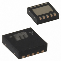
... The MIC5312 is a µCap design, operating with very small ceramic output capacitors for stability, reducing required board space and component cost. The MIC5312 is available in fixed output voltages in the 3mm x 3mm MLF-10 leadless package. Data sheets and support documentation can be found on Micrel’s web site at www ...
Page 2
... IN EN1 2 EN2 3 LOWQ 4 BYP 5 MIC5312-xxBML (3x3) Pin Function Supply Input. (V and V are internally tied together) IN1 IN2 Enable Input (regulator 1). Active High Input. Logic High = On; Logic Low = Off; Do not leave floating Enable Input (regulator 2). Active High Input. Logic High = On; Logic Low = Off; ...
Page 3
Absolute Maximum Ratings Supply Input Voltage (V ) .............................. Enable Input Voltage (V )............................. LowQ™ Input Voltage (V )...................... LowQ™ Power Dissipation (P ) ..................Internally Limited D Junction Temperature ...
Page 4
Electrical Characteristics (LowQ™ Mode 1.0V for higher output of the regulator pair; LowQ™ OUT values indicate -40°C to +125°C, unless noted. Parameter Conditions Output Voltage Accuracy Variation from nominal V Line Regulation ...
Page 5
Typical Characteristics Ripple Rejection vs. I (Normal Mode) LOAD 50mA 40 150mA V =1.85V 30 OUT V =V +1V IN OUT 2.2µF OUT 10nF 300mA BYP 0 10 100 ...
Page 6
Functional Characteristics Enable On- Normal Time (40µs/div) Line Transient - LowQ 5.5V 4V Time (200µs/div) Load Transient - LowQ 10mA 0mA Time (200µs/div) February 2005 I = 200mA LOAD V = 2.6V OUT V = 2.6V OUT ...
Page 7
Functional Characteristics (cont.) Normal to LowQ Transien t Normal LowQ Time (40µs/div) February 2005 10mA LOAD Power-On Reset Characteristics C OUT C SET C BYP LOAD Time (2ms/div) 7 LowQ to Normal Transien t ...
Page 8
... Functional Diagram VIN EN1 TM LOWQ LowQ EN2 BYP Reference February 2005 LDO1 LDO2 GND MIC5312 Block Diagram 8 VOUT1 VOUT2 POR & Delay POR SET M9999-021105 (408) 955-1690 ...
Page 9
... The enable input is CMOS logic and cannot be left floating. There are two regulators in the MIC5312 that share a common bias. Each regulator can be enabled independently by setting the voltage on pins EN1 and EN2 to either logic high or low to turn the channel on or off ...
Page 10
... D(max) D conditions that are critical to the application will give the maximum operating conditions for the regulator circuit. For example, when operating the MIC5312 at 60°C with a minimum footprint layout, the maximum load currents can be calculated as follows: P (max ...
Page 11
Package Information MICREL, INC. 2180 FORTUNE DRIVE SAN JOSE, CA 95131 USA TEL +1 (408) 944-0800 FAX +1 (408) 474-1000 WEB http:/www.micrel.com The information furnished by Micrel in this data sheet is believed to be accurate and reliable. However, no ...