MICRF405YML TR Micrel Inc, MICRF405YML TR Datasheet
MICRF405YML TR
Specifications of MICRF405YML TR
MICRF405YMLTR
MICRF405YMLTR


Related parts for MICRF405YML TR

MICRF405YML TR Summary of contents
Page 1
... MicroLead Frame and MLF are registered trademarks of Amkor Technologies RadioWire is a registered trademark of Micrel, Inc. Micrel Inc. • 2180 Fortune Drive • San Jose, CA 95131 • USA • tel +1 (408) 944-0800 • fax + 1 (408) 474-1000 • http://www.micrel.com April 2006 290MHz – 980MHz ISM Band ...
Page 2
Micrel Table of Contents General Description ................................................................................................................................................................... 1 Features ..................................................................................................................................................................................... 1 Applications................................................................................................................................................................................ 1 Table of Contents....................................................................................................................................................................... 2 Ordering Information .................................................................................................................................................................. 3 Block Diagram............................................................................................................................................................................ 3 Pin Configuration........................................................................................................................................................................ 4 (1) Absolute Maximum Ratings ..................................................................................................................................................... 5 (2) Operating Ratings ................................................................................................................................................................... 5 Electrical Characteristics ...
Page 3
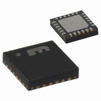
Ordering Information Part Number MICRF405YML ____________________________________________________________________________________________________ Block Diagram April 2006 (1) Junction Temp. Range –40° to +125°C 3 Package ® PB-Free 24-Pin MLF M9999-041906 (408) 955-1690 ...
Page 4
Micrel Pin Configuration Pin Number Pin Name 1 VDD 2 RFGND 3 RFVDD 4 RFOUT 5 RFGND XTB 8 XTA 9 DVDD 10 DGND 11 VDD CLKOUT 14 RDY/DATACLK 15 DATAIN 16 SCK 17 ...
Page 5
Micrel Absolute Maximum Ratings Supply Voltage (V )......................................... +3.7V DD (3) Voltage on any pin (GND = 0V). .. -0.3V to 3.7V Lead Temperature (soldering, 20sec.)............. 260°C Storage Temperature (T ) ................ -55°C to +150°C s (4) ESD Rating All ...
Page 6
Micrel Electrical Characteristics (cont.) Parameter Occupied bandwidth nd 2 Harmonic rd 3 Harmonic Spurious Emission<1GHz Spurious Emission>1GHz LO Leakage Notes: 1. Exceeding the absolute maximum rating may damage the device. 2. The device is not guaranteed to function outside its ...
Page 7
Micrel Data and Configuration Interface The user interface of the MICRF405 is a serial peripheral interface (SPI) consisting of Serial interface enable (SEN), Serial data input/output (SIO) and Serial clock (SCK). This user interface is used for MICRF405 configuration setup ...
Page 8
Micrel Programming Interface Timing Figure 1 and Table 2 shows the timing specification for the 3-wire serial programming interface. Symbol Parameter Tper Min. period of SCK Thigh Min. high time of SCK Tlow Min. low time of SCK Tfall Max. ...
Page 9
Micrel Writing to the Control Registers in MICRF405 Writing: A number of octets are entered into MICRF405 followed by a load-signal to activate the new setting. Making these events is referred “write sequence.” possible to ...
Page 10
Micrel SEN R/W D7 D6D5 SIO SCK In Figure 2, SIO is changed at positive edges of SCK. The MICRF405 samples the SIO line at negative edges. The ...
Page 11
Micrel What to write Field Comments Address: 7 bit = A6, A5, …A0 (A6 = MSB LSB) (address of first byte to write to) R/W bit: “0” for writing Values bits = D7, D6, …D0 (D7 ...
Page 12
Micrel Writing to n Registers having Non-Incremental Addresses Registers with non-incremental addresses can be written to in one write-sequence as well. Example of non-incremental addresses: “0,1,3”. However, this requires more overhead, and the user should consider the possibility to make ...
Page 13
Micrel Data Interface and Data Transfer Adr A6.. 0000000 Mode1=0 Mode0=1 0001100 LowBatt_level=0 LDO_by=0 0001101 Bit_IO_en=1 Manchester_en=0 0011001 SyncID3_7=1 SyncID3_6=1 0011010 SyncID2_7=1 SyncID2_6=1 0011011 SyncID1_7=1 SyncID1_6=1 0011100 SyncID0_7=1 SyncID0_6=1 0011101 DATA_7 DATA_6 There are two main data interfaces; ...
Page 14
Micrel Preamble SyncID 1-4 bytes 1-4 bytes SyncID_Len SynchID_Len Table 8. Virtual Wire Packet Structure, SyncID field. Packet Engine Overview: • Preamble generated by packet engine: 1-4 bytes equal 10101010. Length set ...
Page 15
Micrel How to transmit a Packet with the Packet Engine: Send data CALL PROG [TX] INIT WRITE SEQUENCE [SET SEN=”0"] INIT TX BUFFER [WRITE ADDR 29, R/W =”0"] WRITE FRAME LENGTH PLL IN LOCK? NO [LD=”1"] YES TURN on PA ...
Page 16
Micrel The sequence of a typically packet transfer is shown in Figure 7. 1. Set the 405 in transmit mode with the correct settings by writing in the TX control word. Once SEN is pulled high, the internal load will ...
Page 17
Micrel Programming Summary • Use SEN, SCK, and SIO to get access to the control registers in MICRF405. • SCK is user-controlled. • Write to the MICRF405 on positive edges (MICRF405 reads on negative edges). • Read from the MICRF405 ...
Page 18
Micrel Main Modes of Operation Adr A6..A0 D7 0000000 Mode1=0 There are three main modes of operation and these are controlled by Mode1-0, see Table 9. In “Power down” mode all blocks are shut down, though the contents of the ...
Page 19
Micrel Power level 915MHz (PAx) P (dBm) out 7 10.0 6 5.8 5 3.1 4 0.5 3 -1.9 2 -4.2 1 -6.7 0 -9.2 PA off Table 11. Output Power and Current Consumption vs. Power Level Setting (PA2..PA1) for 315, ...
Page 20
Micrel The frequency synthesizer consists of a voltage- controlled oscillator (VCO), prescaler, programmable frequency dividers, phase- detector and charge pumps. Two different types of prescalers are integrated, a pulse swallow and a phase select prescaler. The recommended prescaler is the ...
Page 21
Micrel Crystal Oscillator (XCO) Adr A6.. 0010101 ClkOut_1=0 ClkOut_0=0 XCO_Fast=1 The crystal oscillator is a very critical block. As the crystal oscillator is a reference for the RF output frequency, very good phase and frequency stability is ...
Page 22
VCO Adr A6.. 0001011 LowBatt_en=1 Freq_Band1=0 0010110 INT_LF_TEST=0 VCO_IB2=0 0011000 VCO_freq_O2 VCO_freq_O1 The VCO has no external components. It oscillates at 1.8 GHz and is divided and 6 in the 900 MHz, 450 MHz or ...
Page 23
Micrel VCO_Fr_Chk Comments 0 VCO control voltage is not controlled VCO control voltage is measured below 0.35V the VC_LO interrupt flag is set higher than 1 AVDD-0.35V the VC_HI flag is set Table 13. ...
Page 24
Micrel Charge Pump and PLL Filter Adr A6.. 0010011 INT_LF_EN=1 CP_CUR1=0 0010100 LF_High_PM=1 LF_CAP1=1 0010110 INT_LF_TEST=0 VCO_IB2=0 There are two charge pumps, one for the external loop filter, and one for the internal filter. Both pumps have four ...
Page 25
Micrel Baud Mod. Freq Rate Coding Type [MHz] [kbaud/ sec] VCO All > 30 Manchester VCO All > 100 Manchester Divider 315 < 20 DC-free Divider 433 < 20 DC-free Divider 868 < 15 DC-free Divider 915 < 20 DC-free ...
Page 26
Modulation Fphd BW type [kHz] [kHz] Open loop 500 22.5 3.125/31.25 VCO Open loop 1000 45 6.25/62.5 VCO ASK 1000 32 3.125/31.25 ≤4.8kbps ASK 2000 64 6.25/62.5 ≤9.6kbps ASK 2000 220 12.5/125 >9.6kbps The design of the PLL filter will ...
Page 27
Micrel Modulation Adr A6.. 0001011 LowBatt_en=1 Freq_Band1=0 0001110 Mod_I4=0 Mod_I3=1 0001111 VCO_Fr_Chk=0 VCO_Fr_Auto=0 0010000 MOD_TEST1=0 Prescaler_Sel=0 0010001 ASK_PN_en=0 ASK_EN=0 0010010 ASKn1=1 ASKn0=0 The frequency modulation can be done in three different ways with the MICRF405, either by closed-, ...
Page 28
Micrel Openloop drift Vdd=3.6V 100 0 -100 -200 -300 -400 -500 -600 -700 -40 - Temperature (degC) Figure 13. Carrier Drift in Open-Loop Modulation. Divider Modulation Modulation[1:0]=2, modulation by switching between two sets of dividers, A0/N0/M0 ...
Page 29
Ref 15 dBm dBm MAXH -10 D2 -19 dBm -20 -30 -40 -50 -60 -70 -80 Center 915 MHz Date: 27.MAR.2006 Figure 14. 33kbps, PA=6, ASK=7, ASKshape=2 (Fphd=2MHz, 209kHz internal loop filter). Spread Spectrum ...
Page 30
Micrel Bit Rate Settings The bit rate is set separately for ASK and FSK modulation to support ASK modulation with FSK spreading. The FSK bit rate is set with the two parameters FSKClk_K and FSKn . The relationship is f ...
Page 31
Micrel The two first blocks are generating a clock for the modulator. This clock is, together with the user data, used to control a charge pump. The charge pump current is controlled by a DAC. Each time the input data ...
Page 32
Micrel Lock Detect Adr A6.. 0001100 LowBatt_level=0 LDO_by=0 0001111 VCO_Fr_Chk=0 VCO_Fr_Auto=0 The lock detector can be enabled by setting LD_en=1. When pin LD is high, it indicates that the PLL is in lock. Care must be taken when ...
Page 33
Low Dropout Regulator (LDO) and Low Battery Detector Adr A6.. 0001011 LowBatt_en=1 Freq_Band1=0 0001100 LowBatt_level=0 LDO_by=0 The MICRF405 has three internal LDOs powering up different parts of the circuit, as can be seen in the Block Diagram. The ...
Page 34
Micrel Bit Description Adr A6.. Mode1=0 Mode0=1 0000000 - - 0000001 - - 0000010 N0_7=0 N0_6=1 0000011 - - 0000100 M0_7=0 M0_6=0 0000101 - - 0000110 - - 0000111 N1_7=0 N1_6=1 0001000 - - 0001001 M1_7=0 M1_6=0 0001010 ...
Page 35
Micrel PA2 PA1 ClkOut_en ClkOut_1 ClkOut_0 Bit_IO_en Sync_en State 0 X DCLK pin on, ...
Page 36
Micrel ASK2 ASK1 ASKshape Comments 0..7 Programmable ASK filter. It can be programmed in eight steps. “0” shaping, “7” most shaping. XCOtune ...
Page 37
Micrel LDO_by LDO_EN1 LDO_EN0 PA_LDc_en Comments only controlled by Mode1 and Mode and PA0- transmit mode (Mode[1:0]=3 and PA[2:0]>0) ...
Page 38
Micrel Pream_Len1 Pream_Len0 Sel_CRC1 Sel_CRC0 Manchester_en Comments 0 Manchester encoding disabled. Manchester encoding enabled. Data will be encoded before transmitted. 1 FSKn > 0 when using ...
Page 39
Micrel MOD_F Comments Programmable smoothing filter after attenuator. This can be programmed in four steps, and will produce 0..3 reasonable results for the highest bit rates. FSKn Comments 0..5 The bit rate clock is set by dividing the crystal oscillator ...
Page 40
Micrel OutS2 OutS1 OutS0 Table 50. Test Signals. Only Available When LD_en=0. PA_IB3 PA_IB2 State 0 ...
Page 41
Micrel LF_RES1<4:0> LF_RES3<4:0> April 2006 R1 (kΩ) 24.1 ...
Page 42
Micrel Typical Application Circuit Bill of Materials FSK/ASK 915MHz Item Part Value Description See Table See Table 3p3 Capacitor, 0603, ±0.25pF, COG, 50V, -55,+125° 100pF Capacitor, 0603, ±5%, ...
Page 43
Micrel FSK/ASK 868MHz Item Part Value Description See Table See Table 3p9 Capacitor, 0603, ±0.25pF, COG, 50V, -55,+125° 15pF Capacitor, 0603, ±5%, COG, 50V, -55,+85° 6p8 ...
Page 44
Micrel FSK/ASK 315MHz Item Part Value Description See Table See Table 10p Capacitor, 0603, ±5%, COG, 50V, -55,+125° 100pF Capacitor, 0603, ±5%, COG, 50V, -55,+85° 10p ...
Page 45
Micrel Package Information ® MLF 4 4x4mm Land pattern E 0.50 Min April 2006 ® 24-Lead MLF (ML 0.30 0.70 3.90 45 MICRF405 3.90 2.55 2.55 M9999-041906 (408) 955-1690 ...
Page 46
Micrel MICREL, INC. 2180 FORTUNE DRIVE SAN JOSE, CA 95131 USA TEL +1 (408) 944-0800 FAX +1 (408) 474-1000 WEB http:/www.micrel.com The information furnished by Micrel in this data sheet is believed to be accurate and reliable. However, no responsibility ...