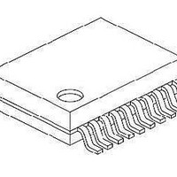
PIC16F1507T-I/SS Microchip Technology, PIC16F1507T-I/SS Datasheet - Page 161

PIC16F1507T-I/SS
Manufacturer Part Number
PIC16F1507T-I/SS
Description
3.5KB Flash, 128B RAM, 18 I/O, CLC, CWG, DDS, 10-bit ADC 20 SSOP .209in T/R
Manufacturer
Microchip Technology
Series
PIC® 16Fr
Datasheets
1.PIC16F1507-EML.pdf
(266 pages)
2.PIC16F1507-EML.pdf
(26 pages)
3.PIC16F1507-EML.pdf
(40 pages)
Specifications of PIC16F1507T-I/SS
Processor Series
PIC16
Core
PIC16F
Data Bus Width
8 bit
Program Memory Type
Flash
Program Memory Size
3.5 KB
Data Ram Size
128 B
Interface Type
ICSP
Maximum Clock Frequency
20 MHz
Number Of Programmable I/os
18
Number Of Timers
3
Operating Supply Voltage
2.3 V to 5.5 V
Maximum Operating Temperature
+ 85 C
Mounting Style
SMD/SMT
Package / Case
SSOP-20
Minimum Operating Temperature
- 40 C
Operating Temperature Range
- 40 C to + 85 C
Supply Current (max)
30 uA
Core Processor
PIC
Core Size
8-Bit
Speed
20MHz
Connectivity
-
Peripherals
Brown-out Detect/Reset, POR, PWM, WDT
Number Of I /o
17
Eeprom Size
-
Ram Size
128 x 8
Voltage - Supply (vcc/vdd)
2.3 V ~ 5.5 V
Data Converters
A/D 12x10b
Oscillator Type
Internal
Operating Temperature
-40°C ~ 85°C
Lead Free Status / Rohs Status
Details
Available stocks
Company
Part Number
Manufacturer
Quantity
Price
Company:
Part Number:
PIC16F1507T-I/SS
Manufacturer:
AD
Quantity:
101
Part Number:
PIC16F1507T-I/SS
Manufacturer:
MICROCHIP/微芯
Quantity:
20 000
- Current page: 161 of 266
- Download datasheet (3Mb)
PIC16(L)F1507
20.0
The Configurable Logic Cell (CLCx) provides program-
mable logic that operates outside the speed limitations
of software execution. The logic cell takes up to 16
input signals and through the use of configurable gates
reduces the 16 inputs to four logic lines that drive one
of eight selectable single-output logic functions.
Input sources are a combination of the following:
• I/O pins
• Internal clocks
• Peripherals
• Register bits
The output can be directed internally to peripherals and
to an output pin.
FIGURE 20-1:
DS41586A-page 161
CLCxIN[10]
CLCxIN[12]
CLCxIN[13]
CLCxIN[14]
CLCxIN[15]
CLCxIN[11]
CLCxIN[0]
CLCxIN[1]
CLCxIN[2]
CLCxIN[3]
CLCxIN[4]
CLCxIN[5]
CLCxIN[6]
CLCxIN[7]
CLCxIN[8]
CLCxIN[9]
CONFIGURABLE LOGIC CELL
(CLC)
See
Figure 20-2
CLCx SIMPLIFIED BLOCK DIAGRAM
lcxg1
lcxg2
lcxg3
lcxg4
See
LCxMODE<2:0>
Function
Figure 20-3
Logic
lcxq
LCxEN
Preliminary
LCxPOL
Refer to
signal flow through the CLCx.
Possible configurations include:
• Combinatorial Logic
• Latches
- AND
- NAND
- AND-OR
- AND-OR-INVERT
- OR-XOR
- OR-XNOR
- S-R
- Clocked D with Set and Reset
- Transparent D with Set and Reset
- Clocked J-K with Reset
Figure 20-1
LCxINTP
LCxINTN
lcx_out
Interrupt
Interrupt
det
det
Q1
for a simplified diagram showing
2011 Microchip Technology Inc.
D
LE
LCxOE
Q
TRIS Control
LCxOUT
MLCxOUT
CLCx
CLCxIF
sets
flag
Related parts for PIC16F1507T-I/SS
Image
Part Number
Description
Manufacturer
Datasheet
Request
R

Part Number:
Description:
3.5KB Flash, 128B RAM, 18 I/O, CLC, CWG, DDS, 10-bit ADC 20 QFN 4x4mm TUBE
Manufacturer:
Microchip Technology
Datasheet:

Part Number:
Description:
3.5KB Flash, 128B RAM, 18 I/O, CLC, CWG, DDS, 10-bit ADC 20 PDIP .300in TUBE
Manufacturer:
Microchip Technology
Datasheet:

Part Number:
Description:
3.5KB Flash, 128B RAM, 18 I/O, CLC, CWG, DDS, 10-bit ADC 20 SOIC .300in TUBE
Manufacturer:
Microchip Technology
Datasheet:

Part Number:
Description:
3.5KB Flash, 128B RAM, 18 I/O, CLC, CWG, DDS, 10-bit ADC 20 SSOP .209in TUBE
Manufacturer:
Microchip Technology
Datasheet:

Part Number:
Description:
3.5KB Flash, 128B RAM, 18 I/O, CLC, CWG, DDS, 10-bit ADC 20 QFN 4x4mm TUBE
Manufacturer:
Microchip Technology
Datasheet:

Part Number:
Description:
3.5KB Flash, 128B RAM, 18 I/O, CLC, CWG, DDS, 10-bit ADC 20 PDIP .300in TUBE
Manufacturer:
Microchip Technology
Datasheet:

Part Number:
Description:
3.5KB Flash, 128B RAM, 18 I/O, CLC, CWG, DDS, 10-bit ADC 20 SOIC .300in TUBE
Manufacturer:
Microchip Technology
Datasheet:

Part Number:
Description:
3.5KB Flash, 128B RAM, 18 I/O, CLC, CWG, DDS, 10-bit ADC 20 SSOP .209in TUBE
Manufacturer:
Microchip Technology
Datasheet:

Part Number:
Description:
Manufacturer:
Microchip Technology Inc.
Datasheet:

Part Number:
Description:
Manufacturer:
Microchip Technology Inc.
Datasheet:

Part Number:
Description:
Manufacturer:
Microchip Technology Inc.
Datasheet:

Part Number:
Description:
Manufacturer:
Microchip Technology Inc.
Datasheet:


