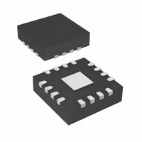
PIC16F526-E/MG Microchip Technology, PIC16F526-E/MG Datasheet - Page 29

PIC16F526-E/MG
Manufacturer Part Number
PIC16F526-E/MG
Description
1.5KB Flash Program, 64B Flash Data, 8MHz Internal Oscillator, 8b ADC, 2x Compar
Manufacturer
Microchip Technology
Series
PIC® 16Fr
Datasheet
1.PIC16F526-ISL.pdf
(122 pages)
Specifications of PIC16F526-E/MG
Core Processor
PIC
Core Size
8-Bit
Speed
20MHz
Peripherals
POR, WDT
Number Of I /o
11
Program Memory Size
1.5KB (1K x 12)
Program Memory Type
FLASH
Ram Size
67 x 8
Voltage - Supply (vcc/vdd)
2 V ~ 5.5 V
Data Converters
A/D 3x8b
Oscillator Type
Internal
Operating Temperature
-40°C ~ 125°C
Package / Case
16-QFN
Lead Free Status / RoHS Status
Lead free / RoHS Compliant
Eeprom Size
-
Connectivity
-
Lead Free Status / RoHS Status
Lead free / RoHS Compliant
- Current page: 29 of 122
- Download datasheet (2Mb)
6.4
The equivalent circuit for an I/O port pin is shown in
Figure 6-1. All port pins, except RB3 which is input-
only, may be used for both input and output operations.
For input operations, these ports are non-latching. Any
input must be present until read by an input instruction
(e.g., MOVF PORTB, W). The outputs are latched and
remain unchanged until the output latch is rewritten. To
use a port pin as output, the corresponding direction
control bit in TRIS must be cleared (= 0). For use as an
input, the corresponding TRIS bit must be set. Any I/O
pin (except RB3) can be programmed individually as
input or output.
2010 Microchip Technology Inc.
I/O Interfacing
FIGURE 6-1:
TRIS ‘f’
Data
Bus
WR
Port
W
Reg
Pin Change
RBPU
Note 1:
COMP
COMP pin Ebl
ADC
ADC pin Ebl
2: Pin enabled as analog for ADC or comparator.
D
D
I/O pins have protection diodes to V
V
CK
CK
RD Port
SS
Reset
Data
Latch
TRIS
Latch
.
(2)
(2)
Q
Q
Q
Q
BLOCK DIAGRAM OF RB0
AND RB1 (with Weak Pull-
up and Wake-up on
Change)
PIC16F526
Q
CK
D
DS41326E-page 29
I/O Pin
DD
and
(1)
Related parts for PIC16F526-E/MG
Image
Part Number
Description
Manufacturer
Datasheet
Request
R

Part Number:
Description:
IC PIC MCU FLASH 1KX12 14SOIC
Manufacturer:
Microchip Technology
Datasheet:

Part Number:
Description:
IC PIC MCU FLASH 1KX12 14DIP
Manufacturer:
Microchip Technology
Datasheet:

Part Number:
Description:
IC PIC MCU FLASH 1KX12 14DIP
Manufacturer:
Microchip Technology
Datasheet:

Part Number:
Description:
IC PIC MCU FLASH 1KX12 14SOIC
Manufacturer:
Microchip Technology
Datasheet:

Part Number:
Description:
1.5KB Flash Program, 64B Flash Data, 8MHz Internal Oscillator, 8b ADC, 2x Compar
Manufacturer:
Microchip Technology
Datasheet:

Part Number:
Description:
1.5KB Flash Program, 64B Flash Data, 8MHz Internal Oscillator, 8b ADC, 2x Compar
Manufacturer:
Microchip Technology
Datasheet:

Part Number:
Description:
1.5KB Flash Program, 64B Flash Data, 8MHz Internal Oscillator, 8b ADC, 2x Compar
Manufacturer:
Microchip Technology
Datasheet:

Part Number:
Description:
IC, 8BIT MCU, PIC16F, 32MHZ, SOIC-18
Manufacturer:
Microchip Technology
Datasheet:

Part Number:
Description:
IC, 8BIT MCU, PIC16F, 32MHZ, SSOP-20
Manufacturer:
Microchip Technology
Datasheet:

Part Number:
Description:
IC, 8BIT MCU, PIC16F, 32MHZ, DIP-18
Manufacturer:
Microchip Technology
Datasheet:

Part Number:
Description:
IC, 8BIT MCU, PIC16F, 32MHZ, QFN-28
Manufacturer:
Microchip Technology
Datasheet:

Part Number:
Description:
IC, 8BIT MCU, PIC16F, 32MHZ, QFN-28
Manufacturer:
Microchip Technology
Datasheet:

Part Number:
Description:
IC, 8BIT MCU, PIC16F, 32MHZ, QFN-28
Manufacturer:
Microchip Technology
Datasheet:

Part Number:
Description:
IC, 8BIT MCU, PIC16F, 32MHZ, SSOP-20
Manufacturer:
Microchip Technology
Datasheet:

Part Number:
Description:
IC, 8BIT MCU, PIC16F, 20MHZ, DIP-40
Manufacturer:
Microchip Technology
Datasheet:


