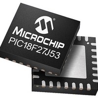
PIC16LF1903-E/MV Microchip Technology, PIC16LF1903-E/MV Datasheet - Page 159

PIC16LF1903-E/MV
Manufacturer Part Number
PIC16LF1903-E/MV
Description
7KB Flash, 256B RAM, LCD, 11x10b ADC, NanoWatt XLP 28 UQFN 4x4x0.5mm TUBE
Manufacturer
Microchip Technology
Series
PIC® XLP™ 16Fr
Datasheet
1.PIC16LF1902-EMV.pdf
(240 pages)
Specifications of PIC16LF1903-E/MV
Processor Series
PIC16LF190x
Core
PIC
Data Bus Width
8 bit
Program Memory Type
Flash
Program Memory Size
4 KB
Data Ram Size
256 B
Maximum Clock Frequency
20 MHz
Number Of Programmable I/os
25
Number Of Timers
2
Operating Supply Voltage
1.8 V to 3.6 V
Maximum Operating Temperature
+ 125 C
Mounting Style
SMD/SMT
Package / Case
QFN-28
Core Processor
PIC
Core Size
8-Bit
Speed
20MHz
Connectivity
-
Peripherals
Brown-out Detect/Reset, LCD, POR, PWM, WDT
Number Of I /o
25
Eeprom Size
-
Ram Size
256 x 8
Voltage - Supply (vcc/vdd)
1.8 V ~ 3.6 V
Data Converters
A/D 11x10b
Oscillator Type
Internal
Operating Temperature
-40°C ~ 125°C
Lead Free Status / Rohs Status
Details
- Current page: 159 of 240
- Download datasheet (3Mb)
18.4.4
The LCD contrast control circuit consists of a
seven-tap resistor ladder, controlled by the LCDCST
bits. Refer to
FIGURE 18-7:
18.4.5
Under firmware control, an internal reference for the
LCD bias voltages can be enabled. When enabled, the
source of this voltage can be either V
one times the main fixed voltage reference (1.024V).
When no internal reference is selected, the LCD con-
trast control circuit is disabled and LCD bias must be
provided externally.
Whenever the LCD module is inactive (LCDA = 0), the
internal reference will be turned off.
When the internal reference is enabled and the Fixed
Voltage Reference is selected, the LCDIRI bit can be
used to minimize power consumption by tieing into the
LCD reference ladder automatic power mode switching.
When LCDIRI = 1 and the LCD reference ladder is in
Power mode ‘B’, the LCD internal FVR buffer is
disables.
2011 Microchip Technology Inc.
Note:
3.072V
From FVR
Buffer
Internal Reference
CONTRAST CONTROL
INTERNAL REFERENCE
The LCD module automatically turns on the
Fixed Voltage Reference when needed.
Figure
V
DDIO
18-7.
INTERNAL REFERENCE AND CONTRAST CONTROL BLOCK DIAGRAM
DDIO
or a voltage
R
Contrast control
Preliminary
R
7 Stages
The contrast control circuit is used to decrease the
output voltage of the signal source by a total of
approximately 10%, when LCDCST = 111.
Whenever the LCD module is inactive (LCDA = 0), the
contrast control ladder will be turned off (open).
18.4.6
The VLCD<3:1> pins provide the ability for an external
LCD bias network to be used instead of the internal lad-
der. Use of the VLCD<3:1> pins does not prevent use
of the internal ladder. Each VLCD pin has an indepen-
dent control in the LCDREF register
allowing access to any or all of the LCD Bias signals.
This architecture allows for maximum flexibility in differ-
ent applications
For example, the VLCD<3:1> pins may be used to add
capacitors to the internal reference ladder, increasing
the drive capacity.
For applications where the internal contrast control is
insufficient, the firmware can choose to only enable the
VLCD3 pin, allowing an external contrast control circuit
to use the internal reference divider.
R
LCDCST<2:0>
VLCD<3:1> PINS
PIC16LF1902/3
R
3
Analog
MUX
7
0
To top of
Reference Ladder
DS41455B-page 159
(Register
18-3),
Related parts for PIC16LF1903-E/MV
Image
Part Number
Description
Manufacturer
Datasheet
Request
R

Part Number:
Description:
IC, 8BIT MCU, PIC16LF, 32MHZ, QFN-28
Manufacturer:
Microchip Technology
Datasheet:

Part Number:
Description:
IC, 8BIT MCU, PIC16LF, 32MHZ, QFN-28
Manufacturer:
Microchip Technology
Datasheet:

Part Number:
Description:
IC, 8BIT MCU, PIC16LF, 32MHZ, DIP-18
Manufacturer:
Microchip Technology
Datasheet:

Part Number:
Description:
IC, 8BIT MCU, PIC16LF, 20MHZ, TQFP-44
Manufacturer:
Microchip Technology
Datasheet:

Part Number:
Description:
7 KB Flash, 384 Bytes RAM, 32 MHz Int. Osc, 16 I/0, Enhanced Mid Range Core, Nan
Manufacturer:
Microchip Technology

Part Number:
Description:
14KB Flash, 512B RAM, LCD, 11x10b ADC, EUSART, NanoWatt XLP 28 SOIC .300in T/R
Manufacturer:
Microchip Technology
Datasheet:

Part Number:
Description:
14KB Flash, 512B RAM, LCD, 11x10b ADC, EUSART, NanoWatt XLP 28 SSOP .209in T/R
Manufacturer:
Microchip Technology
Datasheet:

Part Number:
Description:
MCU PIC 14KB FLASH XLP 28-SSOP
Manufacturer:
Microchip Technology

Part Number:
Description:
MCU PIC 14KB FLASH XLP 28-SOIC
Manufacturer:
Microchip Technology

Part Number:
Description:
MCU PIC 512B FLASH XLP 28-UQFN
Manufacturer:
Microchip Technology

Part Number:
Description:
MCU PIC 14KB FLASH XLP 28-SPDIP
Manufacturer:
Microchip Technology

Part Number:
Description:
MCU 7KB FLASH 256B RAM 40-UQFN
Manufacturer:
Microchip Technology

Part Number:
Description:
MCU 7KB FLASH 256B RAM 44-TQFP
Manufacturer:
Microchip Technology

Part Number:
Description:
MCU 14KB FLASH 1KB RAM 28-UQFN
Manufacturer:
Microchip Technology

Part Number:
Description:
MCU PIC 14KB FLASH XLP 40-UQFN
Manufacturer:
Microchip Technology


