PIC16LF1903T-I/SO Microchip Technology, PIC16LF1903T-I/SO Datasheet - Page 119
PIC16LF1903T-I/SO
Manufacturer Part Number
PIC16LF1903T-I/SO
Description
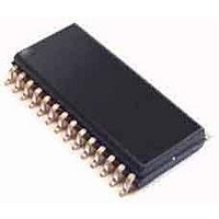
7KB Flash, 256B RAM, LCD, 11x10b ADC, NanoWatt XLP 28 SOIC .300in T/R
Manufacturer
Microchip Technology
Series
PIC® XLP™ 16Fr
Datasheet
1.PIC16LF1902-EMV.pdf
(240 pages)
Specifications of PIC16LF1903T-I/SO
Processor Series
PIC16LF190x
Core
PIC
Data Bus Width
8 bit
Program Memory Type
Flash
Program Memory Size
4 KB
Data Ram Size
256 B
Maximum Clock Frequency
20 MHz
Number Of Programmable I/os
25
Number Of Timers
2
Operating Supply Voltage
1.8 V to 3.6 V
Maximum Operating Temperature
+ 85 C
Mounting Style
SMD/SMT
Package / Case
SOIC-28
Core Processor
PIC
Core Size
8-Bit
Speed
20MHz
Connectivity
-
Peripherals
Brown-out Detect/Reset, LCD, POR, PWM, WDT
Number Of I /o
25
Eeprom Size
-
Ram Size
256 x 8
Voltage - Supply (vcc/vdd)
1.8 V ~ 3.6 V
Data Converters
A/D 11x10b
Oscillator Type
Internal
Operating Temperature
-40°C ~ 85°C
Lead Free Status / Rohs Status
Details


15.2
15.2.1
To enable the ADC module, the ADON bit of the
ADCON0 register must be set to a ‘1’. Setting the
GO/DONE bit of the ADCON0 register to a ‘1’ will start
the Analog-to-Digital conversion.
15.2.2
When the conversion is complete, the ADC module will:
• Clear the GO/DONE bit
• Set the ADIF Interrupt Flag bit
• Update the ADRESH and ADRESL registers with
15.2.3
If a conversion must be terminated before completion,
the GO/DONE bit can be cleared in software. The
ADRESH and ADRESL registers will be updated with
the partially complete Analog-to-Digital conversion
sample. Incomplete bits will match the last bit
converted.
2011 Microchip Technology Inc.
Note:
new conversion result
Note:
ADC Operation
COMPLETION OF A CONVERSION
STARTING A CONVERSION
The GO/DONE bit should not be set in the
same instruction that turns on the ADC.
Refer to
Procedure”.
TERMINATING A CONVERSION
A device Reset forces all registers to their
Reset state. Thus, the ADC module is
turned off and any pending conversion is
terminated.
Section 15.2.5 “A/D Conversion
Preliminary
15.2.4
The ADC module can operate during Sleep. This
requires the ADC clock source to be set to the F
option. When the F
ADC waits one additional instruction before starting the
conversion. This allows the SLEEP instruction to be
executed, which can reduce system noise during the
conversion. If the ADC interrupt is enabled, the device
will wake-up from Sleep when the conversion
completes. If the ADC interrupt is disabled, the ADC
module is turned off after the conversion completes,
although the ADON bit remains set.
When the ADC clock source is something other than
F
sion to be aborted and the ADC module is turned off,
although the ADON bit remains set.
RC
, a SLEEP instruction causes the present conver-
ADC OPERATION DURING SLEEP
PIC16LF1902/3
RC
clock source is selected, the
DS41455B-page 119
RC
Related parts for PIC16LF1903T-I/SO
Image
Part Number
Description
Manufacturer
Datasheet
Request
R

Part Number:
Description:
IC, 8BIT MCU, PIC16LF, 32MHZ, QFN-28
Manufacturer:
Microchip Technology
Datasheet:

Part Number:
Description:
IC, 8BIT MCU, PIC16LF, 32MHZ, QFN-28
Manufacturer:
Microchip Technology
Datasheet:

Part Number:
Description:
IC, 8BIT MCU, PIC16LF, 32MHZ, DIP-18
Manufacturer:
Microchip Technology
Datasheet:

Part Number:
Description:
IC, 8BIT MCU, PIC16LF, 20MHZ, TQFP-44
Manufacturer:
Microchip Technology
Datasheet:
Part Number:
Description:
7 KB Flash, 384 Bytes RAM, 32 MHz Int. Osc, 16 I/0, Enhanced Mid Range Core, Nan
Manufacturer:
Microchip Technology

Part Number:
Description:
14KB Flash, 512B RAM, LCD, 11x10b ADC, EUSART, NanoWatt XLP 28 SOIC .300in T/R
Manufacturer:
Microchip Technology
Datasheet:
Part Number:
Description:
14KB Flash, 512B RAM, LCD, 11x10b ADC, EUSART, NanoWatt XLP 28 SSOP .209in T/R
Manufacturer:
Microchip Technology
Datasheet:
Part Number:
Description:
MCU PIC 14KB FLASH XLP 28-SSOP
Manufacturer:
Microchip Technology
Part Number:
Description:
MCU PIC 14KB FLASH XLP 28-SOIC
Manufacturer:
Microchip Technology
Part Number:
Description:
MCU PIC 512B FLASH XLP 28-UQFN
Manufacturer:
Microchip Technology
Part Number:
Description:
MCU PIC 14KB FLASH XLP 28-SPDIP
Manufacturer:
Microchip Technology

Part Number:
Description:
MCU 7KB FLASH 256B RAM 40-UQFN
Manufacturer:
Microchip Technology
Part Number:
Description:
MCU 7KB FLASH 256B RAM 44-TQFP
Manufacturer:
Microchip Technology

Part Number:
Description:
MCU 14KB FLASH 1KB RAM 28-UQFN
Manufacturer:
Microchip Technology
Part Number:
Description:
MCU PIC 14KB FLASH XLP 40-UQFN
Manufacturer:
Microchip Technology