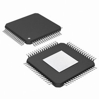
PIC24FJ256DA206T-I/MR Microchip Technology, PIC24FJ256DA206T-I/MR Datasheet - Page 113

PIC24FJ256DA206T-I/MR
Manufacturer Part Number
PIC24FJ256DA206T-I/MR
Description
16-bit, 256KB Flash, 96K RAM, USB, Graphics 64 QFN 9x9x0.9mm T/R
Manufacturer
Microchip Technology
Series
PIC® 24Fr
Specifications of PIC24FJ256DA206T-I/MR
Core Processor
PIC
Core Size
16-Bit
Speed
32MHz
Connectivity
I²C, IrDA, SPI, UART/USART, USB OTG
Peripherals
Brown-out Detect/Reset, GFX, LVD, POR, PWM, WDT
Number Of I /o
52
Program Memory Size
256KB (85.5K x 24)
Program Memory Type
FLASH
Ram Size
96K x 8
Voltage - Supply (vcc/vdd)
2.2 V ~ 3.6 V
Data Converters
A/D 16x10b
Oscillator Type
Internal
Operating Temperature
-40°C ~ 85°C
Package / Case
64-VFQFN, Exposed Pad
Lead Free Status / RoHS Status
Lead free / RoHS Compliant
Eeprom Size
-
Lead Free Status / RoHS Status
Lead free / RoHS Compliant
- Current page: 113 of 408
- Download datasheet (4Mb)
REGISTER 7-15:
2010 Microchip Technology Inc.
bit 15
bit 7
Legend:
R = Readable bit
-n = Value at POR
bit 15
bit 14
bit 13-7
bit 6
bit 5
bit 4-3
bit 2
bit 1
bit 0
Note 1:
U-0
U-0
—
—
If an external interrupt is enabled, the interrupt input must also be configured to an available RPx or RPIx
pin. See Section 10.4 “Peripheral Pin Select (PPS)” for more information.
Unimplemented: Read as ‘0’
RTCIE: Real-Time Clock/Calendar Interrupt Enable bit
1 = Interrupt request is enabled
0 = Interrupt request is not enabled
Unimplemented: Read as ‘0’
INT4IE: External Interrupt 4 Enable bit
1 = Interrupt request is enabled
0 = Interrupt request is not enabled
INT3IE: External Interrupt 3 Enable bit
1 = Interrupt request is enabled
0 = Interrupt request is not enabled
Unimplemented: Read as ‘0’
MI2C2IE: Master I2C2 Event Interrupt Enable bit
1 = Interrupt request is enabled
0 = Interrupt request is not enabled
SI2C2IE: Slave I2C2 Event Interrupt Enable bit
1 = Interrupt request is enabled
0 = Interrupt request is not enabled
Unimplemented: Read as ‘0’
INT4IE
RTCIE
R/W-0
R/W-0
IEC3: INTERRUPT ENABLE CONTROL REGISTER 3
(1)
W = Writable bit
‘1’ = Bit is set
INT3IE
R/W-0
U-0
—
(1)
PIC24FJ256DA210 FAMILY
U-0
U-0
—
—
(1)
(1)
U = Unimplemented bit, read as ‘0’
‘0’ = Bit is cleared
U-0
U-0
—
—
MI2C2IE
R/W-0
U-0
—
x = Bit is unknown
SI2C2IE
R/W-0
U-0
—
DS39969B-page 113
U-0
U-0
—
—
bit 8
bit 0
Related parts for PIC24FJ256DA206T-I/MR
Image
Part Number
Description
Manufacturer
Datasheet
Request
R

Part Number:
Description:
Manufacturer:
Microchip Technology Inc.
Datasheet:

Part Number:
Description:
Manufacturer:
Microchip Technology Inc.
Datasheet:

Part Number:
Description:
Manufacturer:
Microchip Technology Inc.
Datasheet:

Part Number:
Description:
Manufacturer:
Microchip Technology Inc.
Datasheet:

Part Number:
Description:
Manufacturer:
Microchip Technology Inc.
Datasheet:

Part Number:
Description:
Manufacturer:
Microchip Technology Inc.
Datasheet:

Part Number:
Description:
Manufacturer:
Microchip Technology Inc.
Datasheet:

Part Number:
Description:
Manufacturer:
Microchip Technology Inc.
Datasheet:


