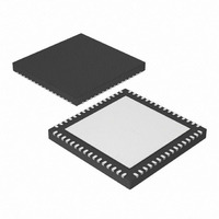
PIC32MX320F064HT-40I/MR Microchip Technology, PIC32MX320F064HT-40I/MR Datasheet - Page 11

PIC32MX320F064HT-40I/MR
Manufacturer Part Number
PIC32MX320F064HT-40I/MR
Description
64 KB Flash, 16 KB RAM, 40 MHz, 10-Bit ADC 64 QFN 9x9x0.9mm T/R
Manufacturer
Microchip Technology
Series
PIC® 32MXr
Datasheets
1.MA320002.pdf
(208 pages)
2.PIC32MX320F032H-40IPT.pdf
(48 pages)
3.PIC32MX320F032H-40IPT.pdf
(66 pages)
4.PIC32MX320F032H-40IPT.pdf
(22 pages)
Specifications of PIC32MX320F064HT-40I/MR
Core Processor
MIPS32® M4K™
Core Size
32-Bit
Speed
40MHz
Connectivity
I²C, IrDA, LIN, PMP, SPI, UART/USART
Peripherals
Brown-out Detect/Reset, POR, PWM, WDT
Number Of I /o
53
Program Memory Size
64KB (64K x 8)
Program Memory Type
FLASH
Ram Size
16K x 8
Voltage - Supply (vcc/vdd)
2.3 V ~ 3.6 V
Data Converters
A/D 16x10b
Oscillator Type
Internal
Operating Temperature
-40°C ~ 85°C
Package / Case
64-VFQFN, Exposed Pad
Processor Series
PIC32MX3xx
Core
MIPS
Data Bus Width
32 bit
Data Ram Size
16 KB
Interface Type
EUART, I2C, SPI
Maximum Clock Frequency
40 MHz
Number Of Programmable I/os
53
Number Of Timers
5
Maximum Operating Temperature
+ 85 C
Mounting Style
SMD/SMT
3rd Party Development Tools
52713-733, 52714-737
Development Tools By Supplier
PG164130, DV164035, DV244005, DV164005, DM320001, DM320002, MA320001
Minimum Operating Temperature
- 40 C
On-chip Adc
10 bit, 16 Channel
Lead Free Status / RoHS Status
Lead free / RoHS Compliant
Eeprom Size
-
Lead Free Status / Rohs Status
Details
25. Module: Input Capture
26. Module: ICSP™
27. Module: UART
© 2010 Microchip Technology Inc.
When in 16-bit mode, the upper 16 bits of the
32-bit ICxBUF register contain Timer3 values.
Work around
Mask the upper 16 bits of the read value.
Example: result = 0xFFFF & IC1BUF
Affected Silicon Revisions
When programming the PIC32 using the 2-wire
PGC and PGD pins, programming data appears
as an output on the JTAG TDO pin.
Work around
Do not connect the TDO pin to a device that would
be adversely affected by rapid pin toggling during
programming.
Affected Silicon Revisions
In BRGH = 1 mode, the received data is not
sampled in the middle of the bit. This reduces the
UART’s baud rate mismatch tolerance.
Work around
Use BRGH = 0 mode.
Affected Silicon Revisions
B2
B2
B2
X
X
X
B3
B3
B3
X
X
X
B4
B4
B4
X
X
X
B6
B6
B6
X
X
X
28. Module: Oscillator
29. Module: ADC
30. Module: Oscillator
A clock signal is present on the CLKO pin,
regardless of the clock source and setting of the
CLOCKOUT Configuration bit, under any of the
following conditions.
1. During a Power-on Reset.
2. During device programming.
3. After a JTAG erase. A clock is present on the
Work around
Do not connect the CLKO pin to a device that
would be adversely affected by rapid pin toggling
or a frequency other than that defined by the
oscillator configuration. Do not use the CLKO pin
as an input if the device connected to the CLKO
pin would be adversely affected by the pin driving
a signal out.
Affected Silicon Revisions
Enabling the primary programming/debug port
(PGC1/PGD1) on 64-lead variants disables the
external and internal references for the ADC,
making the ADC unusable.
Work around
Use the secondary programming/debug port.
Affected Silicon Revisions
After a Fail-Safe Clock Monitor (FSCM) event, the
clock source will be FRC. Firmware clock switch
requests to switch from FRC mode after an FSCM
event may fail. If the clock switch does fail,
subsequent retries by firmware will also fail and
the clock source will be FRC.
Work around
None.
Affected Silicon Revisions
B2
B2
B2
X
X
X
PIC32MX3XX/4XX
CLKO pin until the Configuration bit to disable
CLOCKOUT is programmed.
B3
B3
B3
X
X
X
B4
B4
B4
X
X
X
B6
B6
B6
X
X
X
DS80440D-page 11


