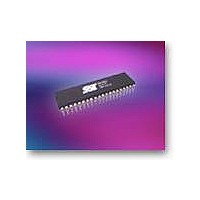
SST89V58RD2-33-I-TQJE Microchip Technology, SST89V58RD2-33-I-TQJE Datasheet - Page 11

SST89V58RD2-33-I-TQJE
Manufacturer Part Number
SST89V58RD2-33-I-TQJE
Description
2.7V To 3.6V FlashFlex 8-bit 8051 Microcontroller 44 TQFP 10x10x1mm TRAY
Manufacturer
Microchip Technology
Series
FlashFlex®r
Datasheet
1.SST89V54RD2-33-C-NJE.pdf
(77 pages)
Specifications of SST89V58RD2-33-I-TQJE
Core Processor
8051
Core Size
8-Bit
Speed
33MHz
Connectivity
EBI/EMI, SPI, UART/USART
Peripherals
Brown-out Detect/Reset, POR, WDT
Number Of I /o
36
Program Memory Size
32KB (32K x 8)
Program Memory Type
FLASH
Eeprom Size
8K x 8
Ram Size
1K x 8
Voltage - Supply (vcc/vdd)
2.7 V ~ 3.6 V
Oscillator Type
External
Operating Temperature
-40°C ~ 85°C
Package / Case
44-TQFP
Processor Series
FlashFlex51
Core
C51
Data Bus Width
8 bit
Data Ram Size
1 KB
Interface Type
SPI
Maximum Clock Frequency
40 MHz
Number Of Programmable I/os
5
Number Of Timers
3
Operating Supply Voltage
2.7 V to 3.6 V
Maximum Operating Temperature
+ 85 C
Mounting Style
SMD/SMT
Minimum Operating Temperature
- 40 C
Lead Free Status / RoHS Status
Lead free / RoHS Compliant
Data Converters
-
Lead Free Status / Rohs Status
Details
Available stocks
Company
Part Number
Manufacturer
Quantity
Price
Company:
Part Number:
SST89V58RD2-33-I-TQJE
Manufacturer:
Microchip Technology
Quantity:
10 000
FlashFlex MCU
SST89V54RD2/RD / SST89V58RD2/RD
3.2 Program Memory Block Switching
The program memory block switching feature of the device allows either Block 1 or the lowest 8 KByte of Block 0 to be
used for the lowest 8 KByte of the program address space. SFCF[1:0] controls program memory block switching.
TABLE
3.2.1 Reset Configuration of Program Memory
Block Switching
Program memory block switching is initialized after reset
according to the state of the Start-up Configuration bit SC0
and/or SC1. The SC0 and SC1 bits are programmed via
an external host mode command or an IAP Mode com-
mand. See Table 4-2.
©2007 Silicon Storage Technology, Inc.
SFCF[1:0]
FIGURE
10, 11
01
00
3-1: SFCF Values for Program Memory Block Switching
FFFFH
0000H
3-2: Program Memory Organization for 32 KByte SST89x58RDx
Program Memory Block Switching
Block 1 is not visible to the PC;
Block 1 is reachable only via in-application programming from E000H - FFFFH.
Both Block 0 and Block 1 are visible to the PC.
Block 0 is occupied from 0000H - 7FFFH. Block 1 is occupied from E000H - FFFFH.
Block 1 is overlaid onto the low 8K of the program address space; occupying address locations 0000H -
1FFFH.
When the PC falls within 0000H - 1FFFH, the instruction will be fetched from Block 1 instead of Block 0.
Outside of 0000H - 1FFFH, Block 0 is used. Locations 0000H - 1FFFH of Block 0 are reachable through
in-application programming.
EA# = 0
64 KByte
External
DFFFH
FFFFH
E000H
7FFFH
1FFFH
8000H
2000H
0000H
SFCF[1:0] = 00
EA# = 1
24 KByte
24 KByte
External
8 KByte
8 KByte
Block 1
Block 0
Block 1
11
DFFFH
FFFFH
7FFFH
E000H
8000H
0000H
Once out of reset, the SFCF[0] bit can be changed dynam-
ically by the program for desired effects. Changing SFCF[0]
will not change the SC0 bit.
SFCF[1:0] = 01
EA# = 1
24 KByte
32 KByte
External
8 KByte
Block 1
Block 0
FFFFH
7FFFH
8000H
0000H
SFCF[1:0] = 10, 11
EA# = 1
32 KByte
32 KByte
External
Block 0
1255 F03.0
S71255-10-000
Data Sheet
T3-1.0 1255
12/07


