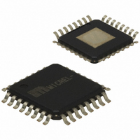
SY69754ALHG Micrel Inc, SY69754ALHG Datasheet - Page 3

SY69754ALHG
Manufacturer Part Number
SY69754ALHG
Description
3.3V 622 Mbps CDR (I Temp, Green/32 Pin TQFP/bulk)
Manufacturer
Micrel Inc
Type
Clock and Data Recovery (CDR)r
Datasheet
1.SY69754ALHG_TR.pdf
(14 pages)
Specifications of SY69754ALHG
Input
PECL, TTL
Output
PECL, TTL
Frequency - Max
1.3GHz
Voltage - Supply
3.15 V ~ 3.45 V
Operating Temperature
-40°C ~ 85°C
Mounting Type
Surface Mount
Package / Case
32-TQFP Exposed Pad, 32-eTQFP, 32-HTQFP, 32-VQFP
Frequency-max
1.3GHz
Lead Free Status / RoHS Status
Lead free / RoHS Compliant
Other names
576-1583
Pin Description
Inputs
Outputs
August 2007
Pin Number
Pin Number
26
32
25
16
31
23
24
20
21
18
17
10
14
15
2
3
5
9
Pin Name
Pin Name
RDOUTN
RDOUTP
DIVSEL1
DIVSEL2
REFCLK
CLKSEL
RCLKN
RCLKP
TCLKP
TCLKN
PLLRN
RDINP
RDINN
PLLSP
PLLSN
PLLRP
LFIN
CD
Differential
Differential
Differential
Differential
TTL Input
TTL Input
TTL Input
Output
PECL
PECL
PECL
PECL
PECL
Type
Type
Input
TTL
Pin Name
Serial Data Input: These built-in line receiver inputs are connected to the
differential receive serial data stream. An internal receive PLL recovers the
embedded clock (RCLK) and data (RDOUT) information.
Reference Clock: This input is used as the reference for the internal frequency
synthesizer and the "training" frequency for the receiver PLL to keep it centered in
the absence of data coming in on the RDIN inputs.
Carrier Detect: This input controls the recovery function of the Receive PLL and
can be driven by the carrier detect output of optical modules or from external
transition detection circuitry. When this input is HIGH, the input data stream
(RDIN) is recovered normally by the Receive PLL. When this input is LOW the
data on the inputs RDIN will be internally forced to a constant LOW, the data
outputs RDOUT will remain LOW, the Link Fault Indicator output LFIN forced
LOW and the clock recovery PLL forced to look onto the clock frequency
generated from REFCLK.
Divider Select: These inputs select the ratio between the output clock frequency
(RCLK/TCLK) and the REFCLK input frequency as shown in the “Reference
Frequency Selection” table.
Clock Select: This input is used to select either the recovered clock of the receiver
PLL (CLKSEL = HIGH) or the clock of the frequency synthesizer (CLKSEL =
LOW) to the TCLK outputs.
Pin Name
Link Fault Indicator: This output indicates the status of the input data stream
RDIN. Active HIGH signal is indicating when the internal clock recovery PLL has
locked onto the incoming data stream. LFIN will go HIGH if CD is HIGH and RDIN
is within the frequency range of the Receive PLL (1000ppm). LFIN is an
asynchronous output.
Receive Data Output: These ECL 100K outputs represent the recovered data
from the input data stream (RDIN). This recovered data is specified against the
rising edge of RCLK.
Clock Output: These ECL 100K outputs represent the recovered clock used to
sample the recovered data (RDOUT).
Clock Output: These ECL 100K outputs represent either the recovered clock
(CLKSEL = HIGH) used to sample the recovered data (RDOUT) or the transmit
clock of the frequency synthesizer (CLKSEL = LOW).
Clock Synthesis PLL Loop Filter: External loop filter pins for the clock synthesis
PLL.
Clock Recovery PLL Loop Filter: External loop filter pins for the receiver PLL.
3
hbwhelp@micrel.com
or (408) 955-1690
M9999-082107-E


