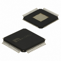
SY87725LHY TR Micrel Inc, SY87725LHY TR Datasheet

SY87725LHY TR
Specifications of SY87725LHY TR
SY87725LHYTR
Related parts for SY87725LHY TR
SY87725LHY TR Summary of contents
Page 1
... Datasheets and support documentation can be found on Micrel’s web site at: www.micrel.com. Micrel Inc. • 2180 Fortune Drive • San Jose, CA 95131 • USA • tel +1 (408) 944-0800 • fax + 1 (408) 474-1000 • http://www.micrel.com July 2007 SY87725L 2.5Gbps GPON/BPON ONU SERDES Features • ...
Page 2
Functional Block Diagram July 2007 2 hbwhelp@micrel.com M9999-071007-B or (408) 955-1690 ...
Page 3
Pin Configuration Ordering Information Package Part Number Type SY87725LHY H64-1 (2) SY87725LHYTR H64-1 Notes: 1. Contact factory for die availability. Dice are guaranteed Tape and Reel. July 2007 6 4-Pin EPAD-TQFP (T64-1) Operating Package Marking Range SY87725LHY ...
Page 4
Pin Description RECEIVE SECTION SIGNALS Pin Number Pin Name 55, 56 SINP, SINN REFCLKP, 60, 61 REFCLKN, 15 REFFREQSEL RCV_PLLRP RCV_PLLRN RCV_PLLSN RCV_PLLSP 59 RCV_SYNC RCV_FSEL0 RCV_FSEL1 39, 40, DOUTOP, DOUT0N, 41, 42, DOUT1P, ...
Page 5
LOOPBACK CONTROLS Pin Number Pin Name XMT_CNTRL0, 16, 17 XMT_CNTRL1 RCV_CNTRL0 RCV_CNTRL1 TRANSLATOR SIGNALS 48 IN 52, 53 OUTP, OUTN POWER PINS AND TEST PIN 13 Testb 20 Test 8 VCCA 9 GNDA 19, 38, 47, 54, VCC ...
Page 6
Functional Description The SY87725L is a fully integrated transceiver with an integrated serial-to-4-bit DeMUX and 4-bit-to-serial Multiplexer. Receive Section Clock and Data Recovery Function The Clock Recovery function includes a synthesizer that generates a stable frequency based on the REFCLK ...
Page 7
Frequency Selections XMT_FSEL0 RCV_FSEL0 XMT_FSEL0 XMT_FSEL1 July 2007 XMT_FSEL1 TX DATA RATE 1244.16Mbps 1 Table 1. Transmit Frequency Selection RCV_FSEL1 RX ...
Page 8
RCV_CNTRL0 RCV_CNTRL1 XMT_CNTRL0 Loop ...
Page 9
Absolute Maximum Ratings Supply Voltage (V ) ................................. –0. 4.6V CC Input Voltage (V )............................................ –0. LVDS Output Current (I )...................................... ±10mA OUT CML Outputs Voltage......................................... V Current ................................................................. ±25mA Lead Temperature (soldering, 20 sec.) ...
Page 10
LVTTL/CMOS DC Electrical Characteristics 3.3V ±5%; GND = GNDA = 0V CCA CCO Symbol Parameter V Input HIGH Voltage IH V Input LOW Voltage IL I Input HIGH Current IH I Input ...
Page 11
AC Electrical Characteristics 3.3V ±5%; GND = GNDA = 0V CCA CCO Symbol Parameter SIN SIN Maximum Data Rate MAX SOUT SOUT Maximum Data Rate MAX t Acquisition Lock Time ACQ Frequency ...
Page 12
Timing Diagrams Receive Timing INTERNAL CLK SIN DOUT0 DOUT1 DOUT2 DOUT3 CLKOUT( ) Normal Mode CLKOUT( ) Half Rate Mode INTERNAL CLK SIN D0 SYNC DOUT0 DOUT1 DOUT2 DOUT3 CLKOUT( ) Normal Mode CLKOUT( ) Half Rate Mode Figure 2. ...
Page 13
Transmit Timing CLKIN (Normal Mode) CLKIN (H alf Rate Mode) DIN0 DIN1 DIN2 DIN3 INTERNAL SERIAL CLK SOUT July 2007 Figure 3. 4:1 Parallel-to-Serial Conversion M9999-071007-B hbwhelp@micrel.com ...
Page 14
Applications Sections This section illustrates the various operating modes of the SY87725L with the appropriate control signals. Normal Data Flow Receive Section The diagram below shows the data paths in a normal operating mode. In this case, downstream data at ...
Page 15
Normal Data Flow (Secondary Clock) Receive Section This mode is identical to the Normal Mode in the RCV_CNTRL0 RCV_CNTRL1 1 RCV_FSEL0 1 July 2007 previous section, but utilizes CLKOUT2 to be used as the transmit parallel clock. In this mode, ...
Page 16
Remote Loopback Mode 00 This is the simplest of the loopback modes as its main purpose is to verify if the link is OK. July 2007 It is possible to combine this with Local Loopback modes; however intended ...
Page 17
Remote Loopback Modes 01 and 10 These modes verify the operation of the CDR by July 2007 looping back the recovered clock or data. The REFCLK is necessary for normal operation of the CDR. Figure 7. Remote Loopback Recovered Clock ...
Page 18
CDR Bypass Mode This mode bypasses the CDR and feeds SIN directly into the DeMUX. Because the CDR is bypassed, there is no recovered clock in this mode. The RefClk is fed directly into the DeMUX and is the serial ...
Page 19
Local Loopback Mode This mode loops the serial data out of the Mux back to the serial input of the DeMux. This allows the July 2007 operation of the Mux and DeMux to be verified through the parallel interface. Figure ...
Page 20
Package Information MICREL, INC. 2180 FORTUNE DRIVE SAN JOSE, CA 95131 USA TEL +1 (408) 944-0800 FAX +1 (408) 474-1000 WEB http:/www.micrel.com The information furnished by Micrel in this data sheet is believed to be accurate and reliable. However, no ...


