USB3311-CP-TR Standard Microsystems (SMSC), USB3311-CP-TR Datasheet
USB3311-CP-TR
Specifications of USB3311-CP-TR
Available stocks


Related parts for USB3311-CP-TR


USB3311-CP-TR Summary of contents
Page 1
... VFBGA lead-free RoHS compliant package also available 0.88mm height) Applications The USB3311 is targeted for any application where a Hi- Speed USB connection is desired and when board space, power, and interface pins must be minimized. The USB3311 is well suited for: ...
Page 2
... USB3311-CP-TR FOR 24 PIN, QFN LEAD-FREE ROHS COMPLIANT PACKAGE (TAPE AND REEL) USB3311-GJ-TR FOR 25 PIN, VFBGA LEAD-FREE ROHS COMPLIANT PACKAGE (TAPE AND REEL) 80 ARKAY DRIVE, HAUPPAUGE, NY 11788 (631) 435-6000, FAX (631) 273-3123 Copyright © 2007 SMSC or its subsidiaries. All rights reserved. Circuit diagrams and other information relating to SMSC products are included as a means of illustrating typical applications. Consequently, complete information sufficient for construction purposes is not necessarily given ...
Page 3
... It is designed to be used in both commercial and industrial temperature applications. The USB3311 meets all of the electrical requirements to be used as a Hi-Speed USB Host, Device On-the-Go (OTG) device. In addition to the supporting USB signaling the USB3311 also provides USB UART mode and USB Audio mode ...
Page 4
... In USB audio mode, the DP pin is shorted to the SPKR_R/M pin with a switch. The DM pin is shorted to the SPKR_L pin. These switches are on when the RESETB pin of the USB3311 is asserted. Audio signals may be transferred over the USB cable. In addition to audio signals, the switches can also be used to connect Full Speed USB from another PHY onto the USB cable ...
Page 5
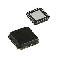
... Hi-Speed USB Transceiver with 1.8V ULPI Interface - 26MHz Reference Clock USB3311 Pin Locations and Descriptions Package Diagram with Pin Locations The pinout below is viewed from the top of the package. ID VBUS VBAT VDD3 Figure 2 USB3311 QFN Pinout - Top View SMSC USB3311 1 18 NXT 2 17 DATA0 3 24Pin QFN ...
Page 6
... Figure 3 USB3311 VFBGA Pinout - Top View Pin Definitions The following table details the pin definitions for the figure above. PIN/ BALL NAME VBUS 3 C2 VBAT Revision 1.3 (11-02-07) Hi-Speed USB Transceiver with 1.8V ULPI Interface - 26MHz Reference Clock TOP VIEW Table 1 USB3311 Pin Description ...
Page 7
... Hi-Speed USB Transceiver with 1.8V ULPI Interface - 26MHz Reference Clock Table 1 USB3311 Pin Description (continued) PIN/ BALL NAME 4 D2 VDD3 SPKR_R SPKR_L 9 D3 DATA[ DATA[ DATA[ DATA[ CLKOUT 14 C4 DATA[ DATA[ DATA[ DATA[ NXT 19 A4 DIR SMSC USB3311 DIRECTION/ ACTIVE TYPE ...
Page 8
... CMOS Analog, N/A Bias Resistor pin. This pin requires an CMOS 8.06kΩ (±1%) resistor to ground, placed as close as possible to the USB3311. Ground N/A Ground. QFN only: The flag should be connected to the ground plane with a via array under the exposed flag. This is the main ground for the IC ...
Page 9
... Battery / Supply USB Connector C VBUS 5 Volt Supply Host Only C Min Max VBUS Host 120uF Device 1uF 10uF OTG Device 1uF 6.5uF Figure 4 USB3311 QFN Application Diagram SMSC USB3311 ID 1 VBUS 2 24 Pin VBAT 3 QFN VDD3 QFN Ground Flag 9 PRODUCT PREVIEW Reference Clock ...
Page 10
... Supply 3.1-5.5V Battery / Supply 8.06KΩ USB Connector C VBUS 5 Volt Supply Host/OTG Only Figure 5 USB3311 VFBGA Application Diagram Revision 1.3 (11-02-07) Hi-Speed USB Transceiver with 1.8V ULPI Interface - 26MHz Reference Clock VDD1.8 B3 VBAT C2 3x3mm VFBGA 25 Ball Array RBIAS A1 0.5mm Pitch ...
Page 11
Package Outlines Figure 6 24-pin QFN, 4x4mm Body, 0.5mm Pitch ...
Page 12
Figure 7 25-pin VFBGA, 3x3mm Body, 0.5mm Pitch ...