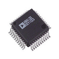
ADV7178KS-REEL Analog Devices Inc, ADV7178KS-REEL Datasheet - Page 16

ADV7178KS-REEL
Manufacturer Part Number
ADV7178KS-REEL
Description
Manufacturer
Analog Devices Inc
Datasheet
1.ADV7178KS-REEL.pdf
(44 pages)
Specifications of ADV7178KS-REEL
Adc/dac Resolution
9b
Screening Level
Commercial
Package Type
MQFP
Pin Count
44
Lead Free Status / RoHS Status
Not Compliant
ADV7177/ADV7178
THEORY OF OPERATION
DATA PATH DESCRIPTION
For PAL B, D, G, H, I, M, N and NTSC M, N modes, YCrCb
4:2:2 data is input via the CCIR-656-compatible pixel port at
a 27 MHz data rate. The pixel data is demultiplexed to form
three data paths. Y typically has a range of 16 to 235, Cr and
Cb typically have a range of 128 ± 112; however, it is possible
to input data from 1 to 254 on both Y, Cb and Cr. The
ADV7177/ADV7178 support PAL (B, D, G, H, I, N, M) and
NTSC (with and without pedestal) standards. The appropriate
SYNC, BLANK , and burst levels are added to the YCrCb data.
Macrovision AntiTaping (ADV7178 only), closed captioning,
OSD (ADV7177 only), and teletext levels are also added to Y,
and the resulting data is interpolated to a rate of 27 MHz. The
interpolated data is filtered and scaled by three digital FIR
filters.
The U and V signals are modulated by the appropriate
subcarrier sine/cosine phases and added together to make up
the chrominance signal. The luma (Y) signal can be delayed
1 to 3 luma cycles (each cycle is 74 ns) with respect to the
chroma signal. The luma and chroma signals are then added
together to make up the composite video signal. All edges are
slew-rate limited.
The YCrCb data is also used to generate RGB data with
appropriate SYNC and BLANK levels. The RGB data is in
synchronization with the composite video output. Alternatively,
analog YUV data can be generated instead of RGB.
The three 9-bit DACs can be used to output:
•
•
•
Alternatively, each DAC can be individually powered off if not
required.
Video output levels are illustrated in the section NTSC
Waveforms With Pedestal.
Internal Filter Response
The Y filter supports several different frequency responses,
including two 4.5 MHz/5.0 MHz low-pass responses, PAL/
NTSC subcarrier notch responses, and a PAL/NTSC extended
response. The U and V filters have a 1.0 MHz/1.3 MHz low-
pass response for NTSC/PAL. These filter characteristics are
illustrated in the Typical Performance Characteristics section.
RGB video
YUV video
One composite video signal + LUMA and CHROMA
(S-video).
Rev. C | Page 16 of 44
Color-Bar Generation
The devices can be configured to generate 100/7.5/75/7.5 color
bars for NTSC or 100/0/75/0 for PAL color bars. These are
enabled by setting MR17 of Mode Register 1 to Logic 1.
Square Pixel Mode
The ADV7177/ADV7178 can be used to operate in square pixel
mode. For NTSC operation, an input clock of 24.5454 MHz is
required. Alternatively, an input clock of 29.5 MHz is required
for PAL operation. The internal timing logic adjusts accordingly
for square pixel mode operation.
Color Signal Control
The color information can be switched on and off the video
output by using Bit MR24 of Mode Register 2.
Burst Signal Control
The burst information can be switched on and off the video
output using Bit MR25 of Mode Register 2.
NTSC Pedestal Control
The pedestal on both odd and even fields can be controlled on a
line-by-line basis by using the NTSC pedestal control registers.
This allows the pedestals to be controlled during the vertical
blanking interval.
PIXEL TIMING DESCRIPTION
The ADV7177/ADV7178 can operate in either 8-bit or 16-bit
YCrCb mode.
8-Bit YCrCb Mode
This default mode accepts multiplexed YCrCb inputs through
the P7 to P0 pixel inputs. The inputs follow the sequence Cb0,
Y0 Cr0, Y1 Cb1, Y2, etc. The Y, Cb and Cr data are input on a
rising clock edge.
16-Bit YCrCb Mode
This mode accepts Y inputs through the P7 to P0 pixel inputs
and multiplexed CrCb inputs through the P15 to P8 pixel
inputs. The data is loaded on every second rising edge of
CLOCK. The inputs follow the sequence Cb0, Y0 Cr0,
Y1 Cb1, Y2, etc.
OSD
The ADV7177 supports OSD. There are twelve, 8-bit OSD
registers loaded with data from the four most significant bits of
Y, Cb, Cr input pixel data bytes. A choice of eight colors can,
therefore, be selected via the OSD_0, OSD_1, OSD_2 pins, each
color being a combination of 12 bits of Y, Cb, Cr pixel data. The
display is under control of the OSD_EN pin. The OSD window
can be an entire screen or just one pixel, and its size may change
by using the OSD_EN signal to control the width on a line-by-
line basis. Figure 5 illustrates OSD timing on the ADV7177.


