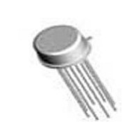
JL198SGA National Semiconductor, JL198SGA Datasheet - Page 6

JL198SGA
Manufacturer Part Number
JL198SGA
Description
Manufacturer
National Semiconductor
Datasheet
1.JL198SGA.pdf
(17 pages)
Specifications of JL198SGA
Number Of Sample And Hold Elements
1
Power Supply Requirement
Dual
Single Supply Voltage (typ)
Not RequiredV
Single Supply Voltage (min)
Not RequiredV
Single Supply Voltage (max)
Not RequiredV
Mounting
Through Hole
Lead Free Status / RoHS Status
Not Compliant
www.national.com
Symbol
TR
en
en
V
I
IB
IO
AC/DC Parameters
Symbol
DC Parameters: Drift Values
Delta calculations performed on S-Level devices at group B, subgroup 5 ONLY.
Note 1: “Absolute Maximum Ratings” indicate limits beyond which damage to the device may occur. Operating Ratings indicate conditions for which the device is
functional, but do not guarantee specific performance limits. For guaranteed specifications and test conditions, see the Electrical Characteristics. The guaranteed
specifications apply only for the test conditions listed. Some performance characteristics may degrade when the device is not operated under the listed test
conditions
Note 2: The maximum power dissipation must be derated at elevated temperatures and is dictated by T
allowable power dissipation at any temperature is P
Note 3: Although the differential voltage may not exceed the limits given, the common-mode voltage on the logic pins may be equal to the supply voltages without
causing damage to the circuit. For proper logic operation, however, one of the logic pins must always be at least 2V below the positive supply and 3V above the
negative supply.
Note 4: Hold step is sensitive to stray capacitive coupling between input logic signals and the hold capacitor. 1 pF, for instance, will create an additional 0.5 mV step
with a 5V logic swing and a 0.01µF hold capacitor. Magnitude of the hold step is inversely proportional to hold capacitor value.
Note 5: Leakage current is measured at a junction temperature of 25˚C. The effects of junction temperature rise due to power dissipation or elevated ambient can
be calculated by doubling the 25˚C value for each 11˚C increase in chip temperature. Leakage is guaranteed over full input signal range.
Note 6: See Definition of Terms
Note 7: Human body model, 100pF discharged through 1.5KΩ
Typical Performance Characteristics
H
S
OS
Parameter
Transient Response
(overshoot)
Noise
Noise
Input Offset Voltage
Input Bias Current
Parameters
Aperture Time
(Note 6)
(Continued)
D
= (T
Conditions
+V
V
+V
V
+V
+V
+V
V
+V
V
JMAX
I
I
CM
CM
20128117
= 100mV pulse
= 100mV pulse
CC
CC
CC
CC
CC
CC
= 0V
= 0V
− T
= 3.5V, -V
= 26.5V, -V
= 15V, -V
= 15V, -V
= 15V, -V
= 15V, -V
A
)/θ
Conditions
JA
, or the number given in the Absolute Maximum Ratings, whichever is lower. .
CC
CC
CC
CC
CC
CC
6
= -15V
= -15V
= -15V,
= -15V,
= -26.5V,
= -3.5V,
Notes
Notes
JMAX
Error in Hold Capacitor
, θ
Dielectric Absorption
JA
, and the ambient temperature, T
Min
Min
-0.5
-2.5
Max
Max
0.5
2.5
40
40
10
10
mV
mV
Unit
Unit
mV
nA
%
%
RMS
RMS
20128118
A
. The maximum
groups
groups
Sub-
Sub-
7
7
7
7
1
1


