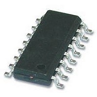
DS90LV031BTM National Semiconductor, DS90LV031BTM Datasheet - Page 3

DS90LV031BTM
Manufacturer Part Number
DS90LV031BTM
Description
01C8071
Manufacturer
National Semiconductor
Datasheet
1.DS90LV031BTM.pdf
(10 pages)
Specifications of DS90LV031BTM
Number Of Elements
4
Input Type
CMOS/TTL
Operating Supply Voltage (typ)
3.3V
Differential Output Voltage
450mV
Propagation Delay Time
2ns
Power Dissipation
1.088W
Operating Temp Range
-40C to 85C
Operating Temperature Classification
Industrial
Mounting
Surface Mount
Pin Count
16
Package Type
SOIC N
Number Of Receivers
4
Number Of Drivers
4
Supply Current
23mA
Supply Voltage Range
3V To 3.6V
Driver Case Style
SOIC
No. Of Pins
16
Operating Temperature Range
-40°C To +85°C
Device Type
Differential Line Driver
Rohs Compliant
No
Data Rate Max
400Mbps
Lead Free Status / RoHS Status
Not Compliant
Available stocks
Company
Part Number
Manufacturer
Quantity
Price
Company:
Part Number:
DS90LV031BTM
Manufacturer:
NS
Quantity:
2
Company:
Part Number:
DS90LV031BTMX
Manufacturer:
NSC
Quantity:
6 613
t
t
t
t
t
t
t
t
t
t
t
t
f
PHLD
PLHD
SKD1
SKD2
SKD3
SKD4
TLH
THL
PHZ
PLZ
PZH
PZL
MAX
Symbol
Switching Characteristics - Industrial
Over supply voltage and operating temperature ranges, unless otherwise specified. (Notes 4, 10, 12)
Note 1: “Absolute Maximum Ratings” are those values beyond which the safety of the device cannot be guaranteed. They are not meant to imply that the devices
should be operated at these limits. The table of “Electrical Characteristics” specifies conditions of device operation.
Note 2: These ABS-MAX voltage ratings are guaranteed by design and bench characterization. The pin under test is pulled negative with respect to ground,
using a curve tracer. During the test, I
Note 3: Current into device pins is defined as positive. Current out of device pins is defined as negative. All voltages are referenced to ground except: V
ΔV
Note 4: All typicals are given for: V
Note 5: The DS90LV031B is a current mode device and only functions within datasheet specifications when a resistive load is applied to the driver outputs typical
range is (90Ω to 110Ω)
Note 6: t
the same channel.
Note 7: t
Note 8: t
specification applies to devices at the same V
Note 9: t
operating temperature and voltage ranges, and across process distribution. t
Note 10: Generator waveform for all tests unless otherwise specified: f = 1 MHz, Z
Note 11: Output short circuit current (I
Note 12: C
Note 13: All input voltages are for one channel unless otherwise specified. Other inputs are set to GND.
Note 14: f
switching.
Parameter Measurement Information
OD1
.
SKD4
SKD1
SKD2
SKD3
MAX
L
Differential Propagation Delay High to Low
Differential Propagation Delay Low to High
Differential Pulse Skew |t
Channel-to-Channel Skew (Note 7)
Differential Part to Part Skew (Note 8)
Differential Part to Part Skew (Note 9)
Rise Time
Fall Time
Disable Time High to Z
Disable Time Low to Z
Enable Time Z to High
Enable Time Z to Low
Maximum Operating Frequency (Note 14)
includes probe and jig capacitance.
, part to part skew, is the differential channel-to-channel skew of any event between devices. This specification applies to devices over recommended
, |t
, Differential Part to Part Skew, is defined as the difference between the minimum and maximum specified differential propagation delays. This
is the Differential Channel-to-Channel Skew of any event on the same device.
generator input conditions: t
PHLD
− t
PLHD
| is the magnitude difference in differential propagation delay time between the positive going edge and the negative going edge of
CC
Parameter
CC
= +3.3V, T
OS
and the current out of the pin under test are monitored using DC meters.
) is specified as magnitude only, minus sign indicates direction only.
r
= t
PHLD
f
CC
< 1ns, (0% to 100%), 50% duty cycle, 0V to 3V. Output Criteria: duty cycle = 45%/55%, VOD > 250mV, all channels
A
and within 5°C of each other within the operating temperature range.
− t
= +25°C.
FIGURE 1. Driver V
PLHD
| (Note 6)
SKD4
R
2 and Figure 3)
R
4 and Figure 5)
OD
L
L
3
= 100Ω, C
= 100Ω, C
and V
is defined as |Max − Min| differential propagation delay.
O
= 50Ω, t
OS
Conditions
Test Circuit
r
L
L
≤
= 10 pF (Figure
= 10 pF (Figure
1 ns, and t
f
≤
1 ns.
10131103
Min
200
0.8
0.8
0
0
0
0
1.18
1.25
0.07
0.38
0.40
Typ
250
0.1
Max
2.0
2.0
0.4
0.5
1.0
1.2
1.5
1.5
5
5
7
7
www.national.com
OD1
Units
MHz
ns
ns
ns
ns
ns
ns
ns
ns
ns
ns
ns
ns
and


