JM38510/13902BIA Analog Devices Inc, JM38510/13902BIA Datasheet - Page 6
JM38510/13902BIA
Manufacturer Part Number
JM38510/13902BIA
Description
Manufacturer
Analog Devices Inc
Datasheet
1.JM3851013902BIA.pdf
(12 pages)
Specifications of JM38510/13902BIA
Number Of Elements
1
Output Type
Single
Power Supply Requirement
Dual
Single Supply Voltage (typ)
Not RequiredV
Single Supply Voltage (min)
Not RequiredV
Single Supply Voltage (max)
Not RequiredV
Dual Supply Voltage (typ)
±15V
Dual Supply Voltage (min)
±8V
Dual Supply Voltage (max)
±22V
Operating Temperature Classification
Military
Mounting
Through Hole
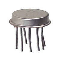
Pin Count
10
Package Type
TO-100
Lead Free Status / RoHS Status
Not Compliant


AD534
A much lower scaling voltage can be achieved without any re-
duction of input signal range using a feedback attenuator as
shown in Figure 4. In this example, the scale is such that V
= XY, so that the circuit can exhibit a maximum gain of 10.
This connection results in a reduction of bandwidth to about
80 kHz without the peaking capacitor C
the output offset voltage is increased by a factor of 10 making
external adjustments necessary in some applications. Adjust-
ment is made by connecting a 4.7 M resistor between Z
the slider of a pot connected across the supplies to provide
Feedback attenuation also retains the capability for adding a
signal to the output. Signals may be applied to the high imped-
ance Z
common ground connection where they are amplified by +1.
Input signals may also be applied to the lower end of the 10 k
resistor, giving a gain of –9. Other values of feedback ratio, up
to X100, can be used to combine multiplication with gain.
Occasionally it may be desirable to convert the output to a cur-
rent, into a load of unspecified impedance or dc level. For ex-
ample, the function of multiplication is sometimes followed by
integration; if the output is in the form of a current, a simple
capacitor will provide the integration function. Figure 5 shows
how this can be achieved. This method can also be applied in
squaring, dividing and square rooting modes by appropriate
choice of terminals. This technique is used in the voltage-
controlled low-pass filter and the differential-input voltage-to-
frequency converter shown in the Applications section.
300 mV of trim range at the output.
X INPUT
Y INPUT
12V PK
12V PK
10V FS
10V FS
Figure 4. Connections for Scale-Factor of Unity
2
terminal where they are amplified by +10 or to the
SF
X
X
Y
Y
1
2
1
2
AD534
OUT
+V
–V
Z
Z
2
S
1
S
–15V
+15V
90k
10k
F
= 200 pF. In addition,
OPTIONAL
PEAKING
CAPACITOR
C
F
= 200pF
OUTPUT ,
= (X
(SCALE = 1V)
1
– X
2
) (Y
12V PK
1
1
– Y
OUT
and
2
)
–6–
OPERATION AS A SQUARER
Operation as a squarer is achieved in the same fashion as the
multiplier except that the X and Y inputs are used in parallel.
The differential inputs can be used to determine the output
polarity (positive for X
of the inputs is reversed). Accuracy in the squaring mode is
typically a factor of 2 better than in the multiplying mode, the
largest errors occurring with small values of output for input
below 1 V.
If the application depends on accurate operation for inputs that
are always less than 3 V, the use of a reduced value of SF is
recommended as described in the Functional Description sec-
tion (previous page). Alternatively, a feedback attenuator may
be used to raise the output level. This is put to use in the differ-
ence-of-squares application to compensate for the factor of 2
loss involved in generating the sum term (see Figure 8).
The difference-of-squares function is also used as the basis for a
novel rms-to-dc converter shown in Figure 15. The averaging
filter is a true integrator, and the loop seeks to zero its input.
For this to occur, (V
is well below the averaging time-constant). Hence V
forced to equal the rms value of V
this technique is very high; at medium frequencies, and for
signals near full scale, it is determined almost entirely by the
ratio of the resistors in the inverting amplifier. The multiplier
scaling voltage affects only open loop gain. The data shown is
typical of performance that can be achieved with an AD534K,
but even using an AD534J, this technique can readily provide
better than 1% accuracy over a wide frequency range, even for
crest-factors in excess of 10.
Y INPUT
X INPUT
10V FS
12V PK
10V FS
12V PK
Figure 5. Conversion of Output to Current
X
X
SF
Y
Y
1
2
1
2
AD534
IN
OUT
+V
–V
)
1
Z
Z
2
2
1
S
= Y
S
– (V
l
and X
OUT
)
CURRENT-SENSING
RESISTOR, R
2
IN
= 0 (for signals whose period
2
. The absolute accuracy of
= Y
I
OUT
2
=
, negative if either one
(X
S
1
, 2k
– X
10V
INTEGRATOR
2
CAPACITOR
) (Y
(SEE TEXT)
MIN
1
– Y
OUT
2
)
REV. B
RS
is
1
Related parts for JM38510/13902BIA
Image
Part Number
Description
Manufacturer
Datasheet
Request
R

Part Number:
Description:
Manufacturer:
Analog Devices Inc
Datasheet:
Part Number:
Description:
Manufacturer:
Analog Devices Inc
Datasheet:

Part Number:
Description:
Manufacturer:
Analog Devices Inc
Datasheet:
Part Number:
Description:
Manufacturer:
Analog Devices Inc
Datasheet:
Part Number:
Description:
Manufacturer:
Analog Devices Inc
Datasheet:
Part Number:
Description:
Manufacturer:
Analog Devices Inc
Datasheet:
Part Number:
Description:
Manufacturer:
Analog Devices Inc
Datasheet:
Part Number:
Description:
Manufacturer:
Analog Devices Inc
Datasheet:
Part Number:
Description:
Manufacturer:
Analog Devices Inc
Datasheet:
Part Number:
Description:
Manufacturer:
Analog Devices Inc
Datasheet:


Part Number:
Description:
TUBE PACK, 300 MIL/N/A/JAN VERSION HA7-2600
Manufacturer:
Intersil Corporation
Part Number:
Description:
28 LD CERDIP/N/A/JAN VERSION HI1-0546
Manufacturer:
Intersil Corporation
Part Number:
Description:
TUBE PACK, 600 MIL/N/A/JAN VERSION HI1-0547
Manufacturer:
Intersil Corporation