AD632SH/883B Analog Devices Inc, AD632SH/883B Datasheet - Page 4
AD632SH/883B
Manufacturer Part Number
AD632SH/883B
Description
Manufacturer
Analog Devices Inc
Datasheet
1.AD632SH883B.pdf
(7 pages)
Specifications of AD632SH/883B
Number Of Elements
1
Output Type
Single
Power Supply Requirement
Dual
Single Supply Voltage (typ)
Not RequiredV
Single Supply Voltage (min)
Not RequiredV
Single Supply Voltage (max)
Not RequiredV
Dual Supply Voltage (typ)
±15V
Dual Supply Voltage (min)
±8V
Dual Supply Voltage (max)
±22V
Operating Temperature Classification
Military
Mounting
Through Hole
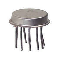
Pin Count
10
Package Type
TO-100
Lead Free Status / RoHS Status
Not Compliant
Available stocks
Company
Part Number
Manufacturer
Quantity
Price


AD632
Typical Performance Curves
(typical @ +25 C with
Figure 3. Frequency Response vs. Divider Denominator
Input Voltage
Figure 2. Frequency Response as a Multiplier
Figure 1. AC Feedthrough vs. Frequency
V
S
= 15 V)
–4–
OPERATION AS A MULTIPLIER
Figure 5 shows the basic connection for multiplication. Note
that the circuit will meet all specifications without trimming.
In some cases the user may wish to reduce ac feedthrough to a
minimum (as in a suppressed carrier modulator) by applying an
external trim voltage (± 30 mV range required) to the X or Y
input. Curve 1 shows the typical ac feedthrough with this ad-
justment mode. Note that the feedthrough of the Y input is a
factor of 10 lower than that of the X input and should be used
in applications where null suppression is critical.
The Z
tional signal into the output. In this mode the output amplifier
behaves as a voltage follower with a 1 MHz small signal band-
width and a 20 V/ s slew rate. This terminal should always be
referenced to the ground point of the driven system, particularly
if this is remote. Likewise the differential inputs should be refer-
enced to their respective signal common potentials to realize the
full accuracy of the AD632.
A much lower scaling voltage can be achieved without any re-
duction of input signal range using a feedback attenuator as
shown in Figure 6. In this example, the scale is such that
V
10. This connection results in a reduction of bandwidth to
about 80 kHz without the peaking capacitor C
output offset voltage is increased by a factor of 10 making exter-
nal adjustments necessary in some applications.
OUT
= XY, so that the circuit can exhibit a maximum gain of
2
terminal of the AD632 may be used to sum an addi-
Figure 4. AD632 Functional Block Diagram
Figure 5. Basic Multiplier Connection
F
. In addition, the
Rev. B
Related parts for AD632SH/883B
Image
Part Number
Description
Manufacturer
Datasheet
Request
R

Part Number:
Description:
IC PREC MULTIPLIER MONO TO100-10
Manufacturer:
Analog Devices Inc
Datasheet:

Part Number:
Description:
Internally Trimmed Precision IC Multiplier
Manufacturer:
Analog Devices
Datasheet:

Part Number:
Description:
±1.7g Dual-Axis IMEMS Accelerometer Evaluation Board
Manufacturer:
Analog Devices Inc
Datasheet:

Part Number:
Description:
Inertial Sensor Evaluation System
Manufacturer:
Analog Devices Inc
Datasheet:
Part Number:
Description:
Manufacturer:
Analog Devices Inc
Datasheet:
Part Number:
Description:
Manufacturer:
Analog Devices Inc
Datasheet:
Part Number:
Description:
Manufacturer:
Analog Devices Inc
Datasheet:
Part Number:
Description:
Manufacturer:
Analog Devices Inc
Datasheet:
Part Number:
Description:
Manufacturer:
Analog Devices Inc
Datasheet:
Part Number:
Description:
Manufacturer:
Analog Devices Inc
Datasheet:
Part Number:
Description:
Manufacturer:
Analog Devices Inc
Datasheet:
Part Number:
Description:
Manufacturer:
Analog Devices Inc
Datasheet:
Part Number:
Description:
Manufacturer:
Analog Devices Inc
Datasheet: