NZF220DFT1G ON Semiconductor, NZF220DFT1G Datasheet

IC FILTER EMI DUAL ESD SOT353

NZF220DFT1G

Manufacturer Part Number
NZF220DFT1G
Description
IC FILTER EMI DUAL ESD SOT353
Manufacturer
ON Semiconductor
Datasheet

Specifications of NZF220DFT1G

Filter Type
Signal Line
Mounting Type
Surface Mount
Termination Style
Surface Mount (SMD,SMT)
Product
EMI Filters
Impedance
50 Ohms
Maximum Dc Current
1 uAmps
Maximum Dc Resistance
110 Ohms
Operating Temperature Range
0 C to + 150 C
Package / Case
SC-70-5
Shielding
Unshielded
Test Frequency
220 MHz
Lead Free Status / RoHS Status
Lead free / RoHS Compliant
Inductance
-
Lead Free Status / Rohs Status
Lead free / RoHS Compliant
Other names
NZF220DFT1GOS
NZF220DFT1GOS
NZF220DFT1GOSTR

Available stocks

Company
Part Number
Manufacturer
Quantity
Price
Part Number:
NZF220DFT1G
Manufacturer:
ON
Quantity:
6 000
Part Number:
NZF220DFT1G
Manufacturer:
ON Semiconductor
Quantity:
188
Part Number:
NZF220DFT1G
Manufacturer:
ON/安森美
Quantity:
20 000
Company:
Part Number:
NZF220DFT1G
Quantity:
6 000
NZF220DFT1
EMI Filter with ESD
Protection
Features
Benefits
Typical Applications
Maximum ratings are those values beyond which device damage can occur.
Maximum ratings applied to the device are individual stress limit values (not
normal operating conditions) and are not valid simultaneously. If these limits are
exceeded, device functional operation is not implied, damage may occur and
reliability may be affected.
1. Between I/O Pins
© Semiconductor Components Industries, LLC, 2005
May, 2005 − Rev. 8
MAXIMUM RATINGS
Peak Power Dissipation (Note 1)
8
Maximum Junction Temperature
Electromagnetic Interference
“Ideal” Low Pass Filtering Response
2 EMI/RFI Bi−directional “Pi” Low−Pass Filters
ESD Protection Meets IEC61000−4−2
Diode Capacitance: 7 − 10 pF
Zener/Resistor Line Capacitance: 22 ±20% pF
Low Zener Diode Leakage: 1 mA Maximum
Zener Breakdown Voltage; 6 − 8 V
Pb−Free Package is Available
Designed to suppress EMI/RFI Noise in Systems Subjected to
Nominal Cutoff Frequency of 220 MHz (per Figure 2)
Small Package Size Minimizes Parasitic Inductance, Thus a More
Cellular Phones
Communication Systems
Computers
Portable Products with Input/Output Conductors
×
20 ms Pulse
Rating
Symbol
P
T
PK
J
Value
150
14
1
Unit
°C
W
NZF220DFT1G
†For information on tape and reel specifications,
NZF220DFT1
including part orientation and tape sizes, please
refer to our Tape and Reel Packaging Specifications
Brochure, BRD8011/D.
Device
ORDERING INFORMATION
FA = Specific Device Code
D = Date Code
G = Pb−Free Package
CIRCUIT DESCRIPTION
Pin 4
Pin 3
MARKING DIAGRAM
http://onsemi.com
(Pb−Free)
Package
SC−88A
SC−88A
1
5
(GND)
FA D
Pin 2
G
2
Publication Order Number:
CASE 419A
DF SUFFIX
SC−88A
4
3
3000/Tape & Reel
3000/Tape & Reel
Pin 5
Pin 1
Shipping
NZF220DFT1/D

Related parts for NZF220DFT1G

NZF220DFT1G Summary of contents

Page 1

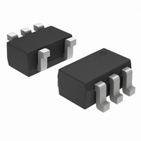
... Between I/O Pins © Semiconductor Components Industries, LLC, 2005 May, 2005 − Rev. 8 Symbol Value Unit °C T 150 J NZF220DFT1 NZF220DFT1G †For information on tape and reel specifications, 1 http://onsemi.com CIRCUIT DESCRIPTION Pin 4 Pin 5 Pin 3 Pin 2 Pin 1 (GND) SC−88A DF SUFFIX CASE 419A MARKING DIAGRAM ...

Page 2

... Use the longest rise/fall times possible for all digital signals Reducing Noise at the Receiver • Filter all I/O signals entering the unit • Locate the I/O filters as close as possible to the connector Minimizing Noise Coupling • Use multilayer PCBs to minimize power and ground inductance • ...

Page 3

NZF220DFT1 FREQUENCY RESPONSE SPECIFICATION TG OUTPUT RF INPUT TEST BOARD NZF220DF Figure 1. Measurement Conditions 0 −6.3 −10 −20 −30 −40 −50 1 FREQUENCY (MHz) Figure 2. Typical EMI Filter Response (50 W Source and 50 W Lead ...

Page 4

... *For additional information on our Pb−Free strategy and soldering details, please download the ON Semiconductor Soldering and Mounting Techniques Reference Manual, SOLDERRM/D. ON Semiconductor and are registered trademarks of Semiconductor Components Industries, LLC (SCILLC). SCILLC reserves the right to make changes without further notice to any products herein. SCILLC makes no warranty, representation or guarantee regarding the suitability of its products for any particular purpose, nor does SCILLC assume any liability arising out of the application or use of any product or circuit, and specifically disclaims any and all liability, including without limitation special, consequential or incidental damages. “ ...

Related keywords