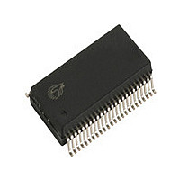
STK17TA8RF45I Cypress Semiconductor Corp, STK17TA8RF45I Datasheet

STK17TA8RF45I
Specifications of STK17TA8RF45I
Related parts for STK17TA8RF45I
STK17TA8RF45I Summary of contents
Page 1
... DQ 7 Note speed in Industrial temperature range is over the operating voltage range of 3.3V+ 0.3V only. Cypress Semiconductor Corporation Document #: 001-52039 Rev. *C 128k X 8 AutoStore nvSRAM with Description The Cypress STK17TA8 combines nonvolatile static RAM (nvSRAM) with a full featured real time clock in a reliable, monolithic integrated circuit ...
Page 2
Contents Features ................................................................................1 Description ...........................................................................1 Logic Block Diagram ...........................................................1 Contents ...............................................................................2 Pinouts .................................................................................3 Pin Descriptions ..................................................................3 Absolute Maximum Ratings ...............................................4 DC Electrical Characteristics .............................................4 AC Test Conditions .............................................................5 Capacitance .........................................................................5 RTC DC Characteristics ......................................................6 SRAM READ Cycles #1 and #2 ...
Page 3
Pinouts V 1 CAP INT (TOP ...
Page 4
Absolute Maximum Ratings Voltage on Input Relative to Ground ................–0.1V to 4.1V Voltage on Input Relative to V .........–0. Voltage HSB.....................–0. 0-7 Temperature under Bias ............................... –55°C to 125°C Junction Temperature ................................... ...
Page 5
DC Electrical Characteristics (V = 2.7V-3.6V) CC Symbol Parameter T Operating Temperature A V Operating Voltage CC V Storage Capacitance CAP NV Nonvolatile STORE operations C DATA Data Retention R AC Test Conditions Input Pulse Levels .................................................... Input ...
Page 6
RTC DC Characteristics Symbol Parameter I RTC Backup Current BAK VRTCbat RTC Battery Pin Voltage VRTCcap RTC Capacitor Pin Voltage tOSCS RTC Oscillator time to start Figure 4. RTC Recommended Component Configuration Document #: 001-52039 Rev. *C Commercial Industrial Units ...
Page 7
SRAM READ Cycles #1 and #2 Symbols NO Alt Chip Enable Access Time ELQV ACS [4] [ Read Cycle Time AVAV ELEH RC [5] [ Address Access ...
Page 8
SRAM WRITE Cycles #1 and #2 Symbols NO Alt Write Cycle Time AVAV AVAV Write Pulse Width WLWH WLEH Chip Enable to End of ...
Page 9
AutoStore/Power Up Recall Symbols NO. Standard Alternate 22 t Power up RECALL Duration HRECALL STORE Cycle Duration STORE HLHZ 24 V Low Voltage Trigger Level SWITCH CCRISE NOTE Read and Write ...
Page 10
Software-Controlled STORE/RECALL Cycle In the following table, the software controlled STORE and RECALL cycle parameters are listed. Symbols NO. E Cont G Cont Alternate AVAV AVAV tAS AVEL AVGL ...
Page 11
Hardware STORE Cycle Symbols NO. Standard Alternate Hardware STORE to SRAM Disabled DELAY HLQZ 32 t Hardware STORE Pulse Width HLHX 32 Soft Sequence Commands NO. Symbols Standard 33 t Soft Sequence Processing Time SS Notes 15. ...
Page 12
MODE Selection Notes 18. The six consecutive addresses must be in the order listed. W must be high during all six consecutive ...
Page 13
Operation The STK17TA8 nvSRAM is made up of two functional compo- nents paired in the same physical cell. These are the SRAM memory cell and a nonvolatile QuantumTrap cell. The SRAM memory cell operates like a standard fast static ...
Page 14
Once a STORE cycle is initiated, further memory inputs and outputs are disabled until the cycle is completed. To initiate the Software STORE cycle, the following read sequence must be performed: 1. Read Address 0x4E38 Valid READ 2. ...
Page 15
Figure 15. Current versus Cycle Time RTC Operations Real Time Clock The clock registers maintain time up to 9,999 years in one second increments. The user can set the time to any calendar time and the clock automatically keeps track ...
Page 16
Calibrating The Clock The RTC is driven by a quartz controlled oscillator with a nominal frequency of 32.768 KHz. Clock accuracy will depend on the quality of the crystal, specified (usually 35 ppm at 25 C). This error could equate ...
Page 17
Interrupts The STK17TA8 has a Flags register, Interrupt Register, and interrupt logic that can interrupt a microcontroller or generate a power up master reset signal. There are three potential interrupt sources: the watchdog timer, the power monitor, and the clock ...
Page 18
RTC Register Register D7 D6 0x1FFFF 10s Years 0x1FFFE 0 0 0x1FFFD 0 0 0x1FFFC 0 0 0x1FFFB 0 0 0x1FFFA 0 10s Minutes 0x1FFF9 0 10s Seconds 0x1FFF8 OSCEN 0 [0] 0x1FFF7 WDS WDW 0x1FFF6 WIE [0] AIE [0] ...
Page 19
Register Map Detail 0x1FFFF D7 D6 10s Years Contains the lower two BCD digits of the year. Lower nibble contains the value for years; upper nibble contains the value for 10s of years. Each nibble operates from ...
Page 20
Register Map Detail (continued) 0x1FFF7 D7 D6 WDS WDW WDS Watchdog Strobe. Setting this bit to 1 reloads and restarts the watchdog timer. The bit is cleared automatically once the watchdog timer is reset. The WDS bit is write only. ...
Page 21
Register Map Detail (continued) 0x1FFF2 Contains the alarm value for the seconds and the mask bit to select or deselect the seconds’ value. M Match. Setting this bit to 0 causes the seconds’ value to be used ...
Page 22
Ordering Information STK17TA8 ITR Ordering Codes These parts are not recommended for new designs. Ordering Code STK17TA8-RF25 3V 128Kx8 AutoStore nvSRAM+RTC SSOP48-300 STK17TA8-RF45 3V 128Kx8 AutoStore nvSRAM+RTC SSOP48-300 STK17TA8-RF25TR 3V 128Kx8 AutoStore nvSRAM+RTC SSOP48-300 STK17TA8-RF45TR 3V 128Kx8 AutoStore ...
Page 23
Package Diagrams Document #: 001-52039 Rev. *C Figure 17. 48-Pin SSOP (51-85061) STK17TA8 51-85061 *D Page [+] Feedback ...
Page 24
... Cypress against all charges. Any Source Code (software and/or firmware) is owned by Cypress Semiconductor Corporation (Cypress) and is protected by and subject to worldwide patent protection (United States and foreign), United States copyright laws and international treaty provisions. Cypress hereby grants to licensee a personal, non-exclusive, non-transferable license to copy, use, modify, create derivative works of, and compile the Cypress Source Code and derivative works for the sole purpose of creating custom software and or firmware in support of licensee product to be used only in conjunction with a Cypress integrated circuit as specified in the applicable agreement ...


