SCDQ5544Q OSRAM Opto Semiconductors Inc, SCDQ5544Q Datasheet - Page 10
SCDQ5544Q
Manufacturer Part Number
SCDQ5544Q
Description
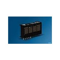
LED Displays 5x5 Hi-Eff Green 0.126 4-CHARACTER
Manufacturer
OSRAM Opto Semiconductors Inc
Series
Intelligent Display®r
Datasheet
1.SCDQ5542P.pdf
(16 pages)
Specifications of SCDQ5544Q
Display Type
Dot Matrix
Emitting Color
Hi-Eff. Green
Number Of Digits
4
Digit Size (in)
.134in
Viewing Area Height (mm)
3.4mm
Viewing Area Length (mm)
3.4mm
Package Type
Panel
Operating Supply Voltage (min)
4.5V
Operating Supply Voltage (typ)
5V
Operating Supply Voltage (max)
5.5V
Operating Temperature Classification
Industrial
Operating Temp Range
-40C to 85C
Mounting
Through Hole
Pin Count
5
Total Thickness (mm)
5.08mm
Opto Display Type
Panel
Pattern Type
Dot Matrix
Millicandela Rating
6.4mcd
Size / Dimension
0.78" L x 0.40" W x 0.20" H (19.91mm x 10.16mm x 5.08mm)
Color
Green
Configuration
5 x 5
Character Size
0.134 in
Illumination Color
High Efficiency Green
Wavelength
568 nm
Maximum Operating Temperature
+ 85 C
Minimum Operating Temperature
- 40 C
Luminous Intensity
6.4 mcd
Viewing Area (w X H)
3.4 mm x 3.4 mm
Lead Free Status / RoHS Status
Compliant
Voltage - Forward (vf) Typ
-
Internal Connection
-
Lead Free Status / Rohs Status
Details
Other names
Q68100A1474Q
Available stocks
Company
Part Number
Manufacturer
Quantity
Price
Company:

Part Number:
SCDQ5544Q
Manufacturer:
MICROCHIP
Quantity:
1 200


Row Strobe Example
The user can activate four Control functions. These include: LED
Brightness Level, Lamp Test, IC Power Down, or Display Clear.
OPCODEs and five bit words are used to initiate these functions.
The OPCODEs and Control Words for the Character Address and
Loading Column Data are shown in Instruction Set Table.
The user can select seven specific LED brightness levels. These
brightness levels (in percentages of full brightness of the display)
include: 100% (F0HEX), 53% (F1HEX), 40% (F2HEX), 27%
(F3HEX), 20% (F4HEX), 13% (F5HEX), and 6.6% (F6HEX). The
brightness levels are controlled by changing the duty factor of the
row strobe pulse.
Display Brightness
Op code
D7 D6 D5
1
1
1
1
1
1
1
The SCDQ554X offers a unique Display Power Down feature
which reduces I
display is set to 0% brightness and the internal multiplex clock is
stopped. When in the Power Down mode data may still be written
into the RAM. The display is reactivated by loading a new right-
ness Level Control Word into the display.
Power Down
Op code
D7 D6 D5
1
2006-05-12
1
1
1
1
1
1
1
1
1
1
1
1
1
1
1
1
Row
Load
SCDQ5541P/Q/R, SCDQ5542P/Q/R, SCDQ5543P/Q/R, SCDQ5544P/Q/R
Control Word
D4
1
1
1
1
1
1
1
Control Word
D4
1
CC
Row 0
Row 1
Row 2
Row 3
Row 4
to less than 50 µA. When FFHEX is loaded the
D3
0
0
0
0
0
0
0
D3
1
0 1 2 3 4
Load Row 0
Columns
D2
D2
0
0
0
0
1
1
1
1
D1
0
0
1
1
0
0
1
D1
1
Row 0
Row 1
Row 2
Row 3
Row 4
D0
0
1
0
1
0
1
0
D0
1
Hex
F0
F1
F2
F3
F4
F5
F6
Hex
FF
0
Load Row 1
Columns
1
2 3
Operation
Level
100%
53%
40%
27%
20%
13%
6.6%
Operation
Level
0%
brightness
4
Row 0
Row 1
Row 2
Row 3
Row 4
10
0
Load Row 2
Columns
The Lamp Test is enabled by loading F8HEX into the serial shift
register. This Control Word sets all of the LEDs to a 53% bright-
ness level. Operation of the Lamp Test has no affect on the RAM
and is cleared by loading a Brightness Control Word.
Lamp Test
Op code
D7 D6 D5
1
1
The Software Clear (C0HEX) clears the Address Register and the
RAM. The display is blanked and the Character Address Register
will be set to Character 0. The internal counter and the Control
Word Register are unaffected. The Software Clear will remain
active until the next data input cycle is initiated.
Software Clear
Op code
D7 D6 D5
1
Electrical & Mechanical Considerations
Interconnect Considerations
Optimum product performance can be had when the following
electrical and mechanical recommendations are adopted. The
SCDQ554XX’s IC is constructed in a high speed CMOS process,
consequently high speed noise on the SERIAL DATA, SERIAL
DATA CLOCK, and LOAD lines may cause incorrect data to be
written into the serial shift register. Adhere to transmission line ter-
mination procedures when using fast line drivers and long cables
(>10 cm).
Good digital grounds (pin 1) and power supply decoupling (pin 2)
will insure that I
erate localized ground bounce. Therefore it is recommended that
each display package use a 0.1 µF and 20 µF capacitor between
V
1
CC
2
1
1
1
and ground.
3
1
1
0
4
Row 0
Row 1
Row 2
Row 3
Row 4
Control Word
D4
1
1
Control Word
D4
0
CC
(<350 mA peak) switching currents do not gen-
0
Load Row 3
D3
0
1
D3
0
Columns
1
2
D2
D2
B
0
0
3 4
D1
B
0
D1
0
Row 0
Row 1
Row 2
Row 3
Row 4
D0
B
0
D0
0
0 1 2
Load Row 4
Columns
Hex
F8
Hex
C0
IDXX5182
3
Operation
Level
Lamp Test
(OFF)
Lamp Test
(ON)
Operation
Level
CLEAR
4
Related parts for SCDQ5544Q
Image
Part Number
Description
Manufacturer
Datasheet
Request
R

Part Number:
Description:
Manufacturer:
OSRAM Opto Semiconductors Inc
Datasheet:

Part Number:
Description:
INTELLIGENT DISP 4CHAR 5X7 HERED
Manufacturer:
OSRAM Opto Semiconductors Inc
Datasheet:

Part Number:
Description:
DISPLAY 8DIGIT CERAMIC GREEN
Manufacturer:
OSRAM Opto Semiconductors Inc
Datasheet:

Part Number:
Description:
EMITTER IR 950NM 5MM SMD RADIAL
Manufacturer:
OSRAM Opto Semiconductors Inc
Datasheet:

Part Number:
Description:
LED TOPLED GREEN 570NM 2-PLCC
Manufacturer:
OSRAM Opto Semiconductors Inc
Datasheet:

Part Number:
Description:
INTERRUPTER RELFECT W/FILTR SMD
Manufacturer:
OSRAM Opto Semiconductors Inc
Datasheet:

Part Number:
Description:
LED Displays 5x7 Green 0.145 , 4-CHARACTER
Manufacturer:
OSRAM Opto Semiconductors Inc
Datasheet:
Part Number:
Description:
Q65110A4321_SIDELED PURE GREEN EOL150407
Manufacturer:
OSRAM Opto Semiconductors Inc
Datasheet:
Part Number:
Description:
Q65110A1202_RO DETECTOR 3/5MM_TR_RO
Manufacturer:
OSRAM Opto Semiconductors Inc
Datasheet:
Part Number:
Description:
INTELLIGENT DISP 4CHAR 5X7 HERED
Manufacturer:
OSRAM Opto Semiconductors Inc
Datasheet:
Part Number:
Description:
LED TOPLED GREEN 570NM 2-PLCC
Manufacturer:
OSRAM Opto Semiconductors Inc
Datasheet:

Part Number:
Description:
PHOTODIODE 900NM 3MM W/FILTER
Manufacturer:
OSRAM Opto Semiconductors Inc
Datasheet:

Part Number:
Description:
PHOTODIODE 850NM THRU-HOLE
Manufacturer:
OSRAM Opto Semiconductors Inc
Datasheet:

Part Number:
Description:
PHOTODIODE 880NM W/FILTER SMD
Manufacturer:
OSRAM Opto Semiconductors Inc
Datasheet: