HFBR-5205A Avago Technologies US Inc., HFBR-5205A Datasheet - Page 2
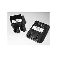
HFBR-5205A
Manufacturer Part Number
HFBR-5205A
Description
Manufacturer
Avago Technologies US Inc.
Datasheet
1.HFBR-5205A.pdf
(23 pages)
Specifications of HFBR-5205A
Optical Fiber Type
TX/RX
Data Transfer Rate
194MBd
Optical Rise Time
3ns
Optical Fall Time
3ns
Jitter
0.04/1ns
Operating Temperature Classification
Commercial
Peak Wavelength
1380/1360nm
Operating Supply Voltage (min)
4.75V
Operating Supply Voltage (typ)
5V
Operating Supply Voltage (max)
5.25V
Output Current
50mA
Operating Temp Range
0C to 70C
Mounting
Through Hole
Pin Count
9
Lead Free Status / RoHS Status
Compliant


Receiver Sections
The receiver sections of the
HFBR-5204 and HFBR-5205
series utilize InGaAs PIN photo-
diodes coupled to a custom
silicon transimpedance preampli-
fier IC. These are packaged in the
optical subassembly portion of
the receiver.
These PIN/preamplifier combina-
tions are coupled to a custom
quantizer IC which provides the
final pulse shaping for the logic
output and the Signal Detect
function. The data output is
differential. The signal detect
output is single-ended. Both data
and signal detect outputs are
PECL compatible, ECL referenced
(shifted) to a +5 volt power
supply.
Package
The overall package concept for
the Agilent transceivers consists
of three basic elements; the two
optical subassemblies, an
electrical subassembly, and the
housing as illustrated in the block
diagrams in Figure 1 and
Figure 1a.
The package outline drawing and
pin out are shown in Figures 2,
2a, and 3. The details of this
package outline and pin out are
compliant with the multisource
definition of the 1x9 SIP. The low
profile of the Agilent transceiver
design complies with the
maximum height allowed for the
duplex SC connector over the
entire length of the package.
Figures 2b and 2c show the
outline drawings for options that
include mezzanine height and
extended and flush shields
respectively.
The optical subassemblies utilize
a high volume assembly process
together with low cost lens
elements which result in a cost
effective building block.
The electrical subassembly con-
sists of a high volume multilayer
printed circuit board on which the
IC chips and various surface-
mounted passive circuit elements
are attached.
The package includes internal
shields for the electrical and
optical subassemblies to insure
low EMI emissions and high
immunity to external EMI fields.
The outer housing including the
duplex SC connector or the
duplex ST ports is molded of filled
non-conductive plastic to provide
mechanical strength and electrical
isolation. The solder posts of the
Agilent design are isolated from
the circuit design of the
transceiver and do not require
DIFFERENTIAL
DATA OUT
SINGLE-ENDED
SIGNAL
DETECT OUT
DIFFERENTIAL
DATA IN
Figure 1. SC Block Diagram.
ELECTRICAL SUBASSEMBLY
QUANTIZER IC
DRIVER IC
2
PREAMP IC
TOP VIEW
connection to a ground plane on
the circuit board.
The transceiver is attached to a
printed circuit board with the nine
signal pins and the two solder
posts which exit the bottom of the
housing. The two solder posts
provide the primary mechanical
strength to withstand the loads
imposed on the transceiver by
mating with the duplex or simplex
SC or ST connectored fiber
cables.
Note: The “T” in the product
numbers indicates a transceiver
with a duplex ST connector
receptacle. Product numbers
without a “T” indicate transceivers
with a duplex SC connector
receptacle.
Application Information
The Applications Engineering
group in the Agilent Optical
Communication Division is
available to assist you with the
technical understanding and
design trade-offs associated with
these transceivers. You can con-
tact them through your Agilent
sales representative.
DUPLEX SC
RECEPTACLE
PIN PHOTODIODE
OPTICAL
SUBASSEMBLIES
LED
Related parts for HFBR-5205A
Image
Part Number
Description
Manufacturer
Datasheet
Request
R

Part Number:
Description:
RECEIVER FIBER OPTIC 600NM 40KBD
Manufacturer:
Avago Technologies US Inc.
Datasheet:

Part Number:
Description:
XMITTER FIBER OPTIC 600NM 5MBD
Manufacturer:
Avago Technologies US Inc.
Datasheet:

Part Number:
Description:
XMITTER FIBER OPTIC 600NM 40KBD
Manufacturer:
Avago Technologies US Inc.
Datasheet:

Part Number:
Description:
XMITTER VERSATILE LINK HORZ
Manufacturer:
Avago Technologies US Inc.
Datasheet:

Part Number:
Description:
XMITTER OPT HI PERFORMANCE VERT
Manufacturer:
Avago Technologies US Inc.
Datasheet:

Part Number:
Description:
TXRX FIBER OPTIC 650NM 10MBAUD
Manufacturer:
Avago Technologies US Inc.
Datasheet:
Part Number:
Description:
TXRX FIBER OPTIC 650NM 10MBAUD
Manufacturer:
Avago Technologies US Inc.
Datasheet:

Part Number:
Description:
FIBER OPTIC TRANSMITTER 660NM
Manufacturer:
Avago Technologies US Inc.
Datasheet:

Part Number:
Description:
KIT EVAL FIBER OPTIC 5MBD
Manufacturer:
Avago Technologies US Inc.
Datasheet:
Part Number:
Description:
KIT EVAL FIBER OPTICS 32MBD
Manufacturer:
Avago Technologies US Inc.
Datasheet:

Part Number:
Description:
KIT EVAL FIBER OPTIC 5MBD
Manufacturer:
Avago Technologies US Inc.
Datasheet:

Part Number:
Description:
125MBd 1300nm FiberOptic Eval Kit
Manufacturer:
Avago Technologies US Inc.
Datasheet:

Part Number:
Description:
DC-5MBd 820nm FiberOptic EvalKit
Manufacturer:
Avago Technologies US Inc.
Datasheet:
Part Number:
Description:
125MBd 820nm FiberOptic Eval Kit
Manufacturer:
Avago Technologies US Inc.
Datasheet:
Part Number:
Description:
DC-5MBd 650nm POF Eval Kit
Manufacturer:
Avago Technologies US Inc.
Datasheet: