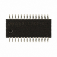
ST1284-01A8 STMicroelectronics, ST1284-01A8 Datasheet - Page 7

ST1284-01A8
Manufacturer Part Number
ST1284-01A8
Description
TERMINATION NETWORK SGL QSOP28
Manufacturer
STMicroelectronics
Series
ASD™r
Type
Network Terminationr
Datasheet
1.ST1284-01A8.pdf
(10 pages)
Specifications of ST1284-01A8
Filter Type
Signal Line
Voltage - Rated
5.5V
Mounting Type
Surface Mount
Termination Style
Surface Mount (SMD,SMT)
Package / Case
QSOP-28
Mounting Style
SMD/SMT
Operating Supply Voltage
5.5 V
Maximum Operating Temperature
+ 70 C
Minimum Operating Temperature
0 C
Lead Free Status / RoHS Status
Lead free / RoHS Compliant
Inductance
-
Lead Free Status / Rohs Status
Lead free / RoHS Compliant
Other names
497-2565-5
Available stocks
Company
Part Number
Manufacturer
Quantity
Price
Part Number:
ST1284-01A8RL
Manufacturer:
ST
Quantity:
20 000
ST1284
To have a good approximation of the remaining voltages at both V
the typical dynamical resistance value R
By taking into account these following hypothesis:
R
The results of the calculation done for V
V
This confirms the very low remaining voltage across the device to be protected. It is also
important to note that in this approximation the parasitic inductance effect was not taken into
account. This could be few tenths of volts during few ns at the input side. This parasitic effect
is not present at the output side due the low current involved after the resistance R.
The measurements done here after show very clearly
ESD protection :
Figure 8.
Figure 9.
BR
t
>R
= 7 V (typ.) and R
–
–
–
–
d
, R
g
V
V
no influence of the parasitic inductances on V
V
strike)
>R
output
output
input
Measurement conditions
Remaining voltage at the input and output of the device during a ±16 kV
ESD surge (IEC 61000-4-2)
d
and R
= 31.2 V
= 7.95 V
clamping voltage very close to V
load
d
= 1 Ω (typ.) give:
>R
SURGE
ESD
d
, it gives these formulas:
Vinput
Voutput
Doc ID 6976 Rev 3
Vinput
=
=
PP
d
R
-------------------------------------------------- -
.
R
--------------------------------------------------------- -
g
= 8 kV, R
t
⋅
ST1284
⋅
V
V
BR
BR
R
+
BR
+
g
R
R
R
t
g
d
(positive strike) and -V
d
⋅
= 330 Ω (IEC 61000-4-2 standard),
⋅
(Figure
V
Vinput
out
PP
stage
Voutput
9) the high efficiency of the
in
and V
Technical information
out
F
stages, we give
(negative
7/10


