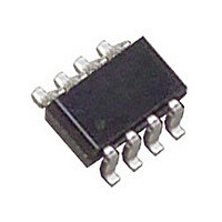
LTC2927CTS8#PBF Linear Technology, LTC2927CTS8#PBF Datasheet - Page 9

LTC2927CTS8#PBF
Manufacturer Part Number
LTC2927CTS8#PBF
Description
Manufacturer
Linear Technology
Datasheet
1.LTC2927CTS8PBF.pdf
(16 pages)
Specifications of LTC2927CTS8#PBF
Operating Temperature (max)
70C
Operating Temperature (min)
0C
Pin Count
8
Mounting
Surface Mount
Package Type
TSOT-23
Case Length
2.9mm
Screening Level
Commercial
Lead Free Status / RoHS Status
Compliant
Available stocks
Company
Part Number
Manufacturer
Quantity
Price
APPLICATIO S I FOR ATIO
Coincident Tracking Example
A typical application is shown in Figure 10. The master
signal is a 3.3V ramp generated by the LTC2927. The
slave 1 supply is a 1.8V switching power supply and the
slave 2 supply is a 2.5V switching power supply. Both
slave supplies track coincidently with the 3.3V ramping
master signal. The ramp rate of the supplies is 100V/s.
The 3-step design procedure detailed previously can be
used to determine component values. Only the slave 1
supply is considered here as the procedure is the same
for the slave 2 supply.
1. Set the ramp rate of the master signal.
2. Solve for the pair of resistors that provide the desired
3. Choose R
From Equation 1:
slave supply behavior, assuming no delay.
From Equation 2:
From Equation 3:
Since no delay is desired, R
R
R
C
TB
TA
RAMP
′ =
=
16 5
=
16 5
1 235
TA
.
.
100
.
10
k
to obtain desired delay.
Ω
k
Ω
μ
V s
V
1V/DIV
•
A
/
U
100
100
+
35 7
1 235
=
0 8
.
V s
V s
0 1
.
.
/
/
.
U
V
k
μ
Ω
V
=
F
16 5
TA
−
16 5
= R
.
0 8
k
W
.
.
10ms/DIV
Ω
TA
k
V
Ω
Figure 9. Coincident Tracking (from Figure 10)
’
≈
13
k
U
Ω
MASTER
SLAVE2
SLAVE1
In this example, the supply remains low while the ON pin
is held below 1.23V. When the ON pin rises above 1.23V,
10μA pulls up the master signal on C
The master signal is buffered from the RAMP pin to the
RAMPBUF pin. As this output and the RAMPBUF pin rise,
the current from the TRACK pin is reduced. Consequently,
the voltage at the slave supply’s output is increased, and
the slave supply tracks the master signal. When the ON
pin is again pulled below 1.23V, 10μA will pull down C
at 100V/s. If the loads on the outputs are suffi cient, all
outputs will track down coincidently at 100V/s.
EARLY V
EARLY
3.3V
3.3V
IN
R
R
16.5k
138k
100k
R
R
887k
412k
R
R
ONB
ONA
13k
TB1
TB2
TA1
TA2
Figure 10. Coincident Tracking Example
10ms/DIV
ON
RAMPBUF
TRACK
ON
RAMPBUF
TRACK
LTC2927
LTC2927
GND
GND
V
V
CC
CC
RAMP
RAMP
SDO
SDO
2927 F10
FB
FB
2927 F09
R
35.7k
R
412k
FA1
FA2
0.1μF
0.1μF
0.1μF
RUN/SS
FB = 1.235V
RUN/SS
FB = 0.8V
1V/DIV
LTC2927
DC/DC
DC/DC
16.5k
R
R
887k
RAMP
3.3V
3.3V
IN
IN
FB1
FB2
OUT
OUT
at 100V/s.
MASTER
3.3V
RAMP
SLAVE1
1.8V
SLAVE2
2.5V
2927fb
9


