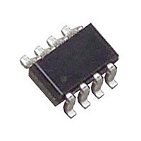
LTC2909ITS8-3.3#PBF Linear Technology, LTC2909ITS8-3.3#PBF Datasheet

LTC2909ITS8-3.3#PBF
Specifications of LTC2909ITS8-3.3#PBF
Available stocks
Related parts for LTC2909ITS8-3.3#PBF
LTC2909ITS8-3.3#PBF Summary of contents
Page 1
... The LTC2909 provides a highly versatile, precise, space- conscious, micropower solution for supply monitoring. , LT, LTC and LTM are registered trademarks of Linear Technology Corporation. All other trademarks are the property of their respective owners. SEL Pin Connection for Input Polarity C ...
Page 2
... LTC2909CDDB-2.5 ADJ2 LTC2909IDDB-2.5 REF LTC2909CDDB-3.3 GND LTC2909IDDB-3.3 LTC2909CDDB-5 LTC2909IDDB ORDER PART NUMBER 8 SEL LTC2909CTS8-2.5 7 TMR 6 V LTC2909ITS8-2 RST LTC2909CTS8-3.3 LTC2909ITS8-3.3 LTC2909CTS8-5 LTC2909ITS8-5 DDB PART* MARKING LBXG LBXG LBZS LBZS LBZT LBZT TS8 PART* MARKING LTBXF LTBXF LTBZV LTBZV LTBZW LTBZW 2909fb ...
Page 3
ELECTRICAL CHARACTERISTICS temperature range, otherwise specifi cations are at T (LTC2909-5), ADJ1 = ADJ2 = 0.55V, SEL = fl oating, unless otherwise noted. (Note 2) SYMBOL PARAMETER V Operating Supply Voltage CC(MIN Shunt Regulation Voltage CC(SHUNT ...
Page 4
LTC2909 W U TYPICAL PERFOR A CE CHARACTERISTICS ADJ Threshold Voltage vs Temperature 508 506 504 502 500 498 496 494 492 – 100 –50 25 TEMPERATURE (°C) 2909 G01 REF Output Load Regulation 1.015 V = ...
Page 5
W U TYPICAL PERFOR A CE CHARACTERISTICS Shunt Regulation Voltage vs Temperature 7.0 6 10mA CC 6 1mA 100μA 6.4 CC 6.2 6.0 50 –50 – 100 TEMPERATURE (°C) 2909 ...
Page 6
LTC2909 CTIO S (TSOT-23/DFN Package) ADJ1 (Pin 1/Pin 8): Adjustable Voltage Input 1. Input to voltage monitor comparator 1 (0.5V nominal threshold). The polarity of the input is selected by the state of the SEL ...
Page 7
W BLOCK DIAGRA CONTROL 2 ADJ1 + – ADJ2 + – – + 500mV – REF DIAGRA S Normal Positive Polarity Input Timing V V ADJ PROP RST ...
Page 8
LTC2909 U U APPLICATIO S I FOR ATIO The LTC2909 is a low power, high accuracy dual/triple supply monitor with two adjustable inputs and an ac- curate UVLO. Reset timeout may be selected with an external capacitor, set to an ...
Page 9
U U APPLICATIO S I FOR ATIO If the state of the SEL pin confi gures a given input as “negative polarity,” the voltage at the ADJx pin must be below the trip point (0.5V nominal), or the ⎯ R ...
Page 10
LTC2909 U U APPLICATIO S I FOR ATIO Table 2b. Possible Combinations of Supply Monitoring. For Example Purposes, All Supplies are Monitored at 5% Tolerance and Connections are Shown Only for ADJ1, ADJ2, REF, SEL 15V (UV/OV 2.37M ...
Page 11
U U APPLICATIO S I FOR ATIO The above discussion is concerned only with the DC value of the monitored supply. Real supplies also have relatively high frequency variation from sources such as load transients, noise and pickup. These variations ...
Page 12
LTC2909 U U APPLICATIO S I FOR ATIO For a positive-monitoring application (2V – TRIP For a negative-monitoring application – TRIP Note that the ...
Page 13
APPLICATIO S I FOR ATIO APPLICATIO S I FOR ATIO Table 3. Suggested Resistor Values for 5% Monitoring 5% UV NOMINAL R VOLTAGE X1 24 232k 10.2M 15 115k 3.09M 12 49.9k 1.07M 9 115k 1.82M ...
Page 14
LTC2909 U U APPLICATIO S I FOR ATIO This imposes a practical limit of 1μF (9 second timeout) if the length of timeout during power-up needs to be longer than 200ms. If the power-up timeout is not important, larger capacitors ...
Page 15
... MOLD FLASH SHALL NOT EXCEED 0.254mm 6. JEDEC PACKAGE REFERENCE IS MO-193 Information furnished by Linear Technology Corporation is believed to be accurate and reliable. However, no responsibility is assumed for its use. Linear Technology Corporation makes no represen- tation that the interconnection of its circuits as described herein will not infringe on existing patent rights. U DDB Package 8-Lead Plastic DFN (3mm × ...
Page 16
... R R GND P1C P1E 51.1k 221k 12V, 3.3V and 2.5V UV DETECT Timing Specifi cations FAIL Pin, RST/ ⎯ R ⎯ S ⎯ T Outputs/Adjustable Reset Timer CC LT 0807 REV B • PRINTED IN USA © LINEAR TECHNOLOGY CORPORATION 2005 SYSTEM R PU2 10k 2909 TA05 2909fb ...


