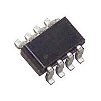
LTC2908CTS8-A1#PBF Linear Technology, LTC2908CTS8-A1#PBF Datasheet - Page 7

LTC2908CTS8-A1#PBF
Manufacturer Part Number
LTC2908CTS8-A1#PBF
Description
Manufacturer
Linear Technology
Datasheet
1.LTC2908CTS8-A1PBF.pdf
(16 pages)
Specifications of LTC2908CTS8-A1#PBF
Voltage Supervisor Type
Voltage Monitor
Number Of Voltage Supervisors
6
Operating Supply Voltage (min)
0.5V
Operating Supply Voltage (max)
6V
Package Type
TSOT-23
Operating Temperature Classification
Commercial
Operating Temp Range
0C to 70C
Pin Count
8
Mounting
Surface Mount
Lead Free Status / RoHS Status
Compliant
Available stocks
Company
Part Number
Manufacturer
Quantity
Price
V2 (Pin 1/Pin 4): Voltage Input 2. The greater of V1, V2 is
also the internal V
not exceed 6V. When in normal operation (V1 > V2), this pin
draws approximately 8μA. When this pin is acting as the
V
this pin to ground with a 0.1μF (or greater) capacitor.
V4 (Pin 2/Pin 3): Voltage Input 4.
RST (Pin 3/Pin 2): Reset Logic Output. Pulls low when
any voltage input is below the reset threshold and is held
low for 200ms after all voltage inputs are above threshold.
This pin has a weak pull-up to V
V
GND (Pin 4/Pin 1): Device Ground.
TYPICAL PERFORMANCE CHARACTERISTICS
PIN FUNCTIONS
Specifi cations are at T
CC
CC
(V2 > V1), this pin draws an additional 16μA. Bypass
using an external pull-up.
–30
–25
–10
–20
–15
3.0
2.5
2.0
1.5
1.0
0.5
–5
0
1.5
0
RST Output Voltage High vs
RST Output Source Current
LTC2908-B1
RST Pull-Up Current vs
Supply Voltage
V1 = 3.3V
V2 = 2.5V
V3 = 1.8V
V4 = 1.5V
V
V
V3 = 2.5V (A1)/V3 = 1.8V (B1)
V4 = 1.8V (A1)/V4 = 1.5V (B1)
V
V
V
RST HELD AT 0V
ADJ1
CC
ADJ1
ADJ1
ADJ5
LTC2908-C1
CC
OUTPUT SOURCE CURRENT, I
2
= V1 = V2 (A1/B1), V
–2
. The operating voltage on this pin shall
= V
A
= V
= V
= 0.55V(C1)
V
= 25°C unless otherwise noted.
SUPPLY VOLTAGE, V
RT25
ADJ2
ADJ2
ADJ2
2.5
–4
= 0.55V
= 0.55V (A1/B1)
= V
ADJ3
3
(TS8 Package/DDB8 Package) LTC2908-A1/LTC2908-B1
–40°C
–6
V
LTC2908-B1
RT33
= V
3.5
CC
CC
ADJ4
LTC2908-A1
= V1(C1)
–8
and may be pulled above
CC
4
=
(V)
RST
V
RT50
25°C
–10
(μA)
4.5
85°C
2908 G22
2908 G20
–12
5
V
for recommended ADJ resistors values.
V3 (Pin 6/Pin 7): Voltage Input 3.
V
for recommended ADJ resistors values.
V1 (Pin 8/Pin 5): Voltage Input 1. The greater of V1, V2 is
also the internal V
not exceed 6V. When in normal operation (V1 > V2), this pin
draws approximately 26 μA. When this pin is not acting as
the V
this pin to ground with a 0.1μF (or greater) capacitor.
Exposed Pad (Pin 9, DDB8 Only): Exposed Pad may be
left open or connected to device ground.
ADJ2
ADJ1
CC
(Pin 5/Pin 8): Adjustable Voltage Input 2. See Table 1
(Pin 7/Pin 6): Adjustable Voltage Input 1. See Table 1
(V2 > V1), this pin draws approximately 8μA. Bypass
2.0
1.0
0.5
1.5
5
4
3
2
1
0
0
RST Output Voltage High vs
RST Output Source Current
LTC2908-A1
RST Output Voltage High vs
RST Output Source Current
LTC2908-C1
V1 = 2.5V
V
V
V1 = 5.0V
V2 = 3.3V
V3 = 2.5V
V4 = 1.8V
V
ADJ1
ADJ4
ADJ1
OUTPUT SOURCE CURRENT, I
CC
OUTPUT SOURCE CURRENT, I
–1
= V
= V
= V
. The operating voltage on this pin shall
–4
ADJ2
ADJ5
–2
ADJ2
= V
= 0.55V
–3
= 0.55V
–8
ADJ3
–40°C
–4
–40°C
=
–12
–5
–6
RST
RST
–16
25°C
85°C
25°C
(μA)
(μA)
–7
85°C
2908 G24
2908 G21
LTC2908
–20
–8
2908fc
7


