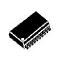
MC100LVEL90DWR2 ON Semiconductor, MC100LVEL90DWR2 Datasheet - Page 4

MC100LVEL90DWR2
Manufacturer Part Number
MC100LVEL90DWR2
Description
Manufacturer
ON Semiconductor
Datasheet
1.MC100LVEL90DWR2.pdf
(6 pages)
Specifications of MC100LVEL90DWR2
Logic Family
ECL
Logical Function
Translator
Technology
ECL
High Level Output Current
-50mA
Low Level Output Current
50mA
Abs. Propagation Delay Time
710ps
Mounting
Surface Mount
Pin Count
20
Operating Temperature (min)
-40C
Operating Temperature (max)
85C
Operating Temperature Classification
Industrial
Lead Free Status / RoHS Status
Not Compliant
Available stocks
Company
Part Number
Manufacturer
Quantity
Price
Company:
Part Number:
MC100LVEL90DWR2
Manufacturer:
MOT
Quantity:
3 512
Part Number:
MC100LVEL90DWR2
Manufacturer:
ON/安森美
Quantity:
20 000
Part Number:
MC100LVEL90DWR2G
Manufacturer:
ON/安森美
Quantity:
20 000
NOTE: Device will meet the specifications after thermal equilibrium has been established when mounted in a test socket or printed circuit
5. Skews are valid across specified voltage range, part−to−part skew is for a given temperature.
6. Duty cycle skew is the difference between a TPLH and TPHL propagation delay through a device.
7. V
Table 5. AC CHARACTERISTICS
Symbol
fmax
t
t
t
tJITTER
V
t
t
PLH
PHL
SKEW
r
f
PP
PP
(min) is swing measured single−ended on each input in differential configuration. The device has a DC gain of ≈40.
board with maintained transverse airflow greater than 500 lfpm. Electrical parameters are guaranteed only over the declared
operating temperature range. Functional operation of the device exceeding these conditions is not implied. Device specification limit
values are applied individually under normal operating conditions and not valid simultaneously.
Maximum Toggle Frequency
Propagation Delay
D to Q
Skew
Random Clock Jitter
Input Voltage Swing (Differential Configuration)
(Note 7)
Output Rise/Fall Times Q
Part−to−Part (Diff) (Note 5)
Output−to−Output (Note 5)
(See Application Note AND8020/D − Termination of ECL Logic Devices.)
Figure 2. Typical Termination for Output Driver and Device Evaluation
Driver
Device
Duty Cycle (Diff) (Note 6)
Characteristic
(20% − 80%)
V
Q
Q
CC
= 3.0 V to 3.8 V; V
S.E.
Diff
Z
Z
http://onsemi.com
o
o
= 50 W
= 50 W
EE
Min
390
340
150
230
= −3.0 V to −5.5 V; GND = 0 V
50 W
V
4
TT
−40°C
560
TBD
Typ
= V
20
25
V
CC
TT
1000
− 2.0 V
Max
590
640
100
200
500
50 W
Min
420
370
150
230
25°C
650
TBD
Typ
D
D
20
25
1000
Max
620
670
100
200
500
Receiver
Device
Min
460
410
150
230
85°C
700
TBD
Typ
20
25
1000
Max
660
710
100
200
500
MHz
ps
Unit
mV
ps
ps
ps


