2N5339JANTX MICROSEMI, 2N5339JANTX Datasheet - Page 2
2N5339JANTX
Manufacturer Part Number
2N5339JANTX
Description
Manufacturer
MICROSEMI
Datasheet
1.2N5339JANTX.pdf
(4 pages)
Specifications of 2N5339JANTX
Transistor Polarity
NPN
Number Of Elements
1
Collector-emitter Voltage
100V
Collector-base Voltage(max)
100V
Emitter-base Voltage (max)
6V
Collector Current (dc) (max)
5A
Dc Current Gain (min)
60
Power Dissipation
1W
Operating Temp Range
-55C to 200C
Operating Temperature Classification
Military
Mounting
Through Hole
Pin Count
3
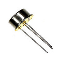
Package Type
TO-39
Lead Free Status / RoHS Status
Not Compliant


6 Lake Street, Lawrence, MA 01841
1-800-446-1158 / (978) 620-2600 / Fax: (978) 689-0803
Website: http://www.microsemi.com
ELECTRICAL CHARACTERISTICS (T
Parameters / Test Conditions
ON CHARACTERISTICS
Forward-Current Transfer Ratio
I
I
I
Collector-Emitter Saturation Voltage
I
I
Base-Emitter Saturation Voltage
I
I
DYNAMIC CHARACTERISTICS
Parameters / Test Conditions
Magnitude of Common Emitter Small-Signal Short-Circuit
Forward Current Transfer Ratio
I
Output Capacitance
V
Input Capacitance
V
SAFE OPERATING AREA
DC Tests
T
Test 1
V
Test 2
V
Test 3
V
(3) Pulse Test: Pulse Width = 300µs, Duty Cycle ≤ 2.0%
T4-LDS-0011 Rev. 3 (101764)
C
C
C
C
C
C
C
C
C
CB
BE
CE
CE
CE
= 0.5Adc, V
= 2.0Adc, V
= 5.0Adc, V
= 2.0Adc, I
= 5.0Adc, I
= 2.0Adc, I
= 5.0Adc, I
= 0.5Adc, V
= +25°C, 1 Cycle, t ≥ 0.5s
= 10Vdc, I
= 2.0Vdc, I
= 2.0Vdc, I
= 5.0Vdc, I
= 90Vdc, I
B
B
B
B
CE
CE
CE
CE
E
C
= 0.2Adc
= 0.5Adc
= 0.2Adc
= 0.5Adc
C
C
C
= 0, 100kHz ≤ f ≤ 1.0MHz
= 55mAdc
= 2.0Vdc
= 2.0Vdc
= 2.0Vdc
= 10Vdc, f = 10MHz
= 0, 100kHz ≤ f ≤ 1.0MHz
= 5.0Adc
= 2.0Adc
(3)
A
= +25°C, unless otherwise noted) (CONT.)
TECHNICAL DATA SHEET
Symbol
Symbol
V
V
C
C
h
CE(sat)
BE(sat)
|h
FE
obo
ibo
fe
|
Gort Road Business Park, Ennis, Co. Clare, Ireland
Tel: +353 (0) 65 6840044 Fax: +353 (0) 65 6822298
Min.
Min.
60
60
40
3.0
Max.
Max.
1,000
240
250
0.7
1.2
1.2
1.8
15
Page 2 of 4
Unit
Unit
Vdc
Vdc
pF
pF
Related parts for 2N5339JANTX
Image
Part Number
Description
Manufacturer
Datasheet
Request
R

Part Number:
Description:
NPN Power Silicon Switching Transistor
Manufacturer:
Microsemi Corporation

Part Number:
Description:
MICROSEMI DIODE
Manufacturer:
MICROSEMI
Datasheet:
Part Number:
Description:
Schottky Rectifier
Manufacturer:
Microsemi Corporation
Datasheet:
Part Number:
Description:
Schottky Rectifier
Manufacturer:
Microsemi Corporation
Datasheet:
Part Number:
Description:
Schottky Rectifier
Manufacturer:
Microsemi Corporation
Datasheet:
Part Number:
Description:
Schottky Rectifier
Manufacturer:
Microsemi Corporation
Datasheet:
Part Number:
Description:
Ultra Fast Rectifier (less than 100ns)
Manufacturer:
Microsemi Corporation
Datasheet:
Part Number:
Description:
Manufacturer:
Microsemi Corporation
Datasheet:
Part Number:
Description:
Ultra Fast Rectifier (less than 100ns)
Manufacturer:
Microsemi Corporation
Datasheet:
Part Number:
Description:
Ultra Fast Rectifier (less than 100ns)
Manufacturer:
Microsemi Corporation
Datasheet:
Part Number:
Description:
Manufacturer:
Microsemi Corporation
Datasheet:
Part Number:
Description:
Manufacturer:
Microsemi Corporation
Datasheet:
Part Number:
Description:
Manufacturer:
Microsemi Corporation
Datasheet:
Part Number:
Description:
Manufacturer:
Microsemi Corporation
Datasheet:
Part Number:
Description:
Manufacturer:
Microsemi Corporation
Datasheet: