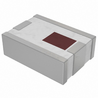
2450BP15B100E Johanson Technology Inc, 2450BP15B100E Datasheet - Page 55

2450BP15B100E
Manufacturer Part Number
2450BP15B100E
Description
FILTER BANDPASS 2.4GHZ
Manufacturer
Johanson Technology Inc
Specifications of 2450BP15B100E
Frequency
2.45GHz Center
Bandwidth
100MHz
Filter Type
Bandpass
Insertion Loss
2.2dB
Package / Case
0805 (2012 Metric)
Mounting Type
Surface Mount
Frequency Range
2.4GHz To 2.5GHz
Return Loss
9.5dB
Bandpass Insertion Loss Max
2.2dB
Attenuation @ Reject Band Min
10dB
Filter Case
0805
Termination Type
SMD
Rohs Compliant
Yes
Lead Free Status / RoHS Status
Lead free by exemption / RoHS Compliant
Ripple
-
Other names
2450BP15B100
712-1078-2
712-1078-2
significant; third digit
CODE
M10 = 1.0” x 1.0”
M12 = 1.2” x 1.2”
M15 = 1.5” x 1.5”
M20 = 2.0” x 2.0”
etc...
denotes number of
6R0 = 6VDCW
250 = 25 VDCW
101 = 100 VDCW
501 = 500 VDCW
102 = 1000 VDCW
502 = 5000 VDCW
T
H
1st two digits are
VOLTAGE CODE
zeros, R denotes
Use size codes
for dimension
SIZE CODES
decimal point.
M = Substrate
OW TO
PART TYPE
500
DIM.
O
RDER
M
W
12
DIELECTRIC CODE
A = NPO/COG
B = BX/X7R
C = NPO
D = BX
F = ALUMINUM/
G = ALUMINA
K = NPO
L = NEG TC
N = NPO
Q = P90/Hi Q
R = NEG TC
T = X7R
U = NEG TC
V = NEG TC
W = X7R
X = X7R
Y = Y5V
Z = Z5U
eg: 050 = 5.0 mils
eg: 065 = 6.5 mils
eg: 128 = 12.8 mils
Thickness in mils
3rd digit is the
decimal point
NITRIDE
THICKNESS
CODE
T
045
www.johansontechnology.com
K
A or Blank = Not applicable
S = Seed layer gold only
P = 100 micro” min. std
X = Special
Use blank in the S column
instead of “A” only if it the
last character in the part#
X = Unterminated
9 = Thick film
G = Thick film + Au
H = Thick film + Ni-Au
T = Thin Film TiW-AU
N = Thin Film TiW-NI-AU
R = TaN-TiW-Au
V = TiW-Ni-Sn
E = 80Au/20Sn
C = TiW-Ni-Cu-Ni-Au
S = Special
TOLERANCE
THICKNESS
A = ± 0.5 mil
B = ± 1.0 mil
C = ± 2.0 mil
J = ± 5.0 %
K = ± 10.0 %
L = ± 15.0 %
M = ± 20.0 %
X = Special
metalization code
CODE
GS = Back side
METALIZATION
L
G
Optional Metallization,
Top, Bottom, or Both Sides
S
A or Blank = Not applicable
S = Seed layer gold only
P = 100 micro” min. std
X = Special
Leave R and T blank if both
sides have the same type
metalization.
If metalization types are
different, then back side is
scribed with an X.
X = Unterminated
9 = Thick film
G = Thick film + Au
H = Thick film + Ni-Au
T = Thin Film TiW-AU
N = Thin Film TiW-NI-AU
R = TaN-TiW-Au
V = TiW-Ni-Sn
E = 80Au/20Sn
C = TiW-Ni-Cu-Ni-Au
S = Special
Blank = Both Sides are the
Same
metalization code
FLATNESS (Standard): 1 mil per 100 mils.
Please contact the factory for other flatness
options.
NOTE: The thickness specified in the JTI
part number is the thickness of the dielectric
material not including the termination
materials.
NOTE: The standard thickness of the Nickel
barrier (if used) is 10 - 20 microinches
(for non-bordered parts) and is 20 - 50
microinches (for bordered parts), and the
thickness of the Gold is 100 microinches
minimum.
thicknesses are available upon request.
METALIZATION
RT = Top side
R
-
Other termination material
T
***
cust, code, non-std. thk.,
NON-STANDARD CODE
product marking, lead-
ing, testing, dielectric,
Defines non-standard
L, W, endband & size
-
*** - ASTERISK
Required (place
codes,etc...
holders)
AA
55


