www.RFM.com E-mail: info@rfm.com
©2009 by RF Monolithics, Inc.
Electrical Characteristics
Electrical Connections
1.
2.
3.
4.
• Designed for WLAN IF Applications
• Low Insertion Loss
• 5.0 x 5.0 x 1.7 mm Suface-Mount Case
• Differential or Single Ended Input and Output
• Complies with Directive 2002/95/EC (RoHS)
Absolute Maximum Ratings
Differential Input / Output Impedance Match
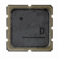
Case Style
Lid Symbolization (Y=year, WW=week, S=shift)
Port 1 Hot
Port 1 Gnd Return
Port 2 Hot
Port 2 Gnd Return
Case Ground
Rating
Maximum Incident Power in Passband
Maximum DC Voltage Between any Two Terminals
Storage Temperature Range
Suitable for lead-free soldering - Maximum Soldering Profile
Characteristic
Nominal Center Frequency
Passband
Rejection
Operating Temperature Range
Unless noted otherwise, all specifications apply over the operating temper-
ature range with filter soldered to the specified demonstration board with
impedance matching to 50 Ω and measured with 50 Ω network analyzer.
Unless noted otherwise, all frequency specifications are referenced to the
nominal center frequency, fc.
Rejection is measured as attenuation below the minimum IL point in the
passband. Rejection in final user application is dependent on PCB layout
and external impedance matching design. See Application Note No. 42
for details.
"LRIP" or "L" after the part number indicates "low rate initial production"
and "ENG" or "E" indicates "engineering prototypes."
Connection
CAUTION: Electrostatic Sensitive Device. Observe precautions for handling.
Notes:
Amplitude Ripple over fc ±7.0 MHz
Group Delay Variation over fc ±7.0
Terminals
All others
2
3
6
7
fc +16.5 to fc +22 MHz
fc +43 to fc +100 MHz
fc -22 to fc -16.5 MHz
fc -100 to fc -33 MHz
fc +22 to fc +43 MHz
fc -33 to fc -22 MHz
Insertion Loss at fc
3 dB Passband
Pb
100
100
Sym
GDV
BW
RF IC
-40 to +85
T
f
IL
C
Value
A
5.
6.
7.
8.
3
+10
30
260°C for 30 s
The design, manufacturing process, and specifications of this filter are
subject to change.
Either Port 1 or Port 2 may be used for either input or output in the design.
However, impedances and impedance matching may vary between Port 1
and Port 2, so that the filter must always be installed in one direction per
the circuit design.
US and international patents may apply.
RFM, stylized RFM logo, and RF Monolithics, Inc. are registered
trademarks of RF Monolithics, Inc.
27nH
Notes
1, 2, 3
1, 2
12pf
12pf
1
1
SM5050-8 5 X 5 mm Nominal Footprint
Units
VDC
dBm
°C
pin 3
Min
pin 2
-10
17
45
40
30
30
35
40
SAW Filter
TOP VIEW
External L-C
447, YWWS
374.000
pin 7
pin 6
Typ
8.7
0.8
23
61
54
53
40
44
48
49
374.00 MHz
SAW Filter
SF1174B
SM5050-8
12pf
12pf
Max
10.0
+85
27nH
100
1.0
SF1174B - 3/16/09
RF IC
Page 1 of 3
Units
dB
ns
200
MHz
MHz
dB
dB
°C
P-P
P-P