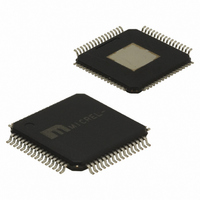
SY87702LHI Micrel Inc, SY87702LHI Datasheet - Page 6

SY87702LHI
Manufacturer Part Number
SY87702LHI
Description
IC CLOCK/DATA RECOVERY 64-TQFP
Manufacturer
Micrel Inc
Type
Clock and Data Recovery (CDR)r
Datasheet
1.SY87702LHI.pdf
(14 pages)
Specifications of SY87702LHI
Input
Differential
Output
Differential
Frequency - Max
325MHz
Voltage - Supply
3.15 V ~ 3.45 V
Operating Temperature
-40°C ~ 85°C
Mounting Type
Surface Mount
Package / Case
64-TQFP Exposed Pad, 64-eTQFP, 64-HTQFP, 64-VQFP
Frequency-max
325MHz
Lead Free Status / RoHS Status
Contains lead / RoHS non-compliant
Micrel, Inc.
FREQSEL1, ..., FREQSEL3 [Frequency Select] – TTL
Inputs
shown in Table 2.
frequency (RCLK/TCLK) and the REFCLK input frequency
as shown in Table 3. Please note that the divide by 32
selection, “011”, is only available for use when FREQSEL
are set to “000.”
CLKSEL [Clock Select] – TTL Input
the receiver PLL (CLKSEL = HIGH) or the clock of the
frequency synthesizer (CLKSEL = LOW) to the TCLK
outputs.
ENPECL [Enable PECL] – TTL Input
differential PECL outputs TCLKE± RDOUTE±, and RCLKE±.
It also disables the CML outputs, by setting TCLKC+,
RDOUTC+, and RCLKC+ logic HIGH and setting TCLKC–,
RDOUTC–, and RCLKC– logic LOW.
differential CML outputs TCLKC±, RDOUTC±, and RCLKC±.
It also disables the PECL outputs by setting TCLKE+,
RDOUTE+, and RCLKE+ logic HIGH and setting TCLKE–,
RDOUTE–, and RCLKE– logic LOW.
M9999-072706
hbwhelp@micrel.com or (408) 955-1690
DIVSEL1, ..., DIVSEL3 [Divider Select] – TTL Inputs
FREQSEL1
These inputs select the output clock frequency range, as
These inputs select the ratio between the output clock
This input is used to select either the recovered clock of
This input, when HIGH (ENPECL = 1), enables the
When set LOW (ENPECL = 0), this signal enables the
DIVSEL1
0
0
0
0
1
1
1
1
0
0
0
0
1
1
1
1
FREQSEL2
DIVSEL2
0
0
1
1
0
0
1
1
0
0
1
1
0
0
1
1
Table 2.
Table 3.
FREQSEL3
DIVSEL3
0
1
0
1
0
1
0
1
0
1
0
1
0
1
0
1
REFCLK
VCOCLK
Multiplier
Divider
32
10
16
20
12
16
24
1
2
4
8
1
2
4
6
8
6
OUTPUTS
LFIN [Link Fault Indicate] – O.C. TTL Output
RDIN. LFIN will go HIGH if CD is HIGH and RDIN is within
the frequency range of the Receive PLL (as per ALRSEL).
LFIN is an asynchronous output.
RDOUTE
from the input data stream (RDIN). This recovered data is
sampled on the falling edge of RCLK.
RDOUTC
RCLKE
used to sample the recovered data (RDOUT).
RCLKC
TCLKE
clock (CLKSEL = HIGH) used to sample the recovered data
(RDOUT) or the transmit clock of the frequency synthesizer
(CLKSEL = LOW).
TCLKC
INPUTS/OUTPUTS
PLLSN+, PLLSN– [Clock Synthesis Loop Filter]
band PLL.
PLLSW+, PLLSW– [Clock Synthesis Loop Filter]
PLLs.
PLLRN+, PLLRN– [Clock Recovery Loop Filter]
band PLL.
PLLRW+, PLLRW– [Clock Recovery Loop Filter]
PLLs.
OTHERS
VCC
VCCO
VCCA
GND
GNDA
NC
This output indicates the status of the input data stream
These ECL 100K outputs represent the recovered data
This is the CML version of RDOUTE±.
These ECL 100K outputs represent the recovered clock
This is the CML version of RCLKE±.
These ECL 100K outputs represent either the recovered
This is the CML version of TCLKE±.
External loop filter pins for the clock synthesis narrow-
External loop filter pins for the clock synthesis wide-band
External loop filter pins for the clock recovery narrow-
External loop filter pins for the clock recovery wide-band
±
±
±
±
[Transmit Clock Out] – Differential PECL
±
±
[Receive Clock Out] – Differential PECL
[Transmit Clock Out] – Differential CML
[Receive Clock Out] – Differential CML
Supply Voltage
Output Supply Voltage
Analog Supply Voltage
Ground
Analog Ground
These pins are for factory test, and are to be
left unconnected during normal use.
[Receive Data Out] – Differential PECL
[Receive Data Out] – Differential CML
SY87702L


