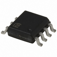
SY100EL11VZG Micrel Inc, SY100EL11VZG Datasheet - Page 7

SY100EL11VZG
Manufacturer Part Number
SY100EL11VZG
Description
IC FANOUT BUFFER 1:2 DIFF 8-SOIC
Manufacturer
Micrel Inc
Series
100EL, Precision Edge®r
Type
Fanout Buffer (Distribution)r
Datasheet
1.SY100EL11VZG_TR.pdf
(8 pages)
Specifications of SY100EL11VZG
Number Of Circuits
1
Ratio - Input:output
1:2
Differential - Input:output
Yes/Yes
Input
Clock
Output
Clock
Voltage - Supply
3 V ~ 5.5 V
Operating Temperature
-40°C ~ 85°C
Mounting Type
Surface Mount
Package / Case
8-SOIC (3.9mm Width)
No. Of Outputs
2
Supply Current
150µA
Supply Voltage Range
-3V To -5.5V
Digital Ic Case Style
SOIC
No. Of Pins
8
Operating Temperature Range
-40°C To +85°C
Termination Type
SMD
Supply Voltage Max
5V
Lead Free Status / RoHS Status
Lead free / RoHS Compliant
Frequency-max
-
Lead Free Status / RoHS Status
Lead free / RoHS Compliant, Lead free / RoHS Compliant
Other names
576-3518-5
SY100EL11VZG
SY100EL11VZG
Available stocks
Company
Part Number
Manufacturer
Quantity
Price
Company:
Part Number:
SY100EL11VZG
Manufacturer:
MICREL
Quantity:
75 540
Part Number:
SY100EL11VZGTR
Manufacturer:
MICREL/麦瑞
Quantity:
20 000
Micrel, Inc.
V
V
V
Notes:
1.
2.
3.
4.
5.
M9999-052610
hbwhelp@micrel.com or (408) 955-1690
Symbol
t
t
t
t
t
t
PLH
PHL
skew
JITTER
r
f
EE
PP
CMR
AC ELECTRICAL CHARACTERISTICS
= V
EE
Parametric values specified at:
Within-device skew defined as identical transitions on similar paths through a device.
Duty cycle skew is the difference between a tPLH and tPHL propagation delay through a device.
Minimum input swing for which AC parameters are guaranteed. The device has a DC gain of 40.
The CMR range is referenced to the most positive side of the differential input signal. Normal operation is obtained if the HIGH level falls
within the specified range and the peak-to-peak voltage lies between VPP min. and 1V. The lower end of the CMR range varies 1:1 with VEE.
The numbers in the spec table assume a nominal VEE = –3.3V. Note for PECL operation, the VCMR (min) will be fixed at 3.3V – |VCMR
(min)|.
Propagation Delay to
Output D
Within-Device Skew
Duty Cycle Skew
Random Clock Jitter (RMS)
Minimum Input Swing
Common Mode Range
Output Rise/Fall Times Q
(20% to 80%)
(Min.) to V
Parameter
EE
(Max.); V
(3)
(2)
(4)
(5)
CC
Min.
–1.3
135
150
100
= GND
—
—
—
T
10/100EL11V Series:
A
Typ.
260
225
= –40°C
—
—
—
5
5
Max.
–0.4
385
350
—
—
—
—
(1)
Min.
–1.4
185
150
100
—
—
—
T
7
A
Typ.
260
225
= 0°C
—
—
—
5
5
-3.0V to -5.5V.
Max.
–0.4
335
350
20
20
—
—
Min.
–1.4
190
150
100
—
—
—
T
A
= +25°C
Typ.
265
225
0.6
—
—
5
5
Max.
–0.4
340
350
20
20
—
—
Min.
–1.4
215
150
100
—
—
—
T
A
Typ.
290
225
= +85°C
—
—
—
5
5
Max.
SY100EL11V
–0.4
365
350
20
20
—
—
SY10EL11V
Unit
mV
ps
ps
ps
ps
V


