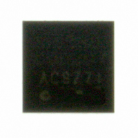
SI5330C-A00207-GM Silicon Laboratories Inc, SI5330C-A00207-GM Datasheet

SI5330C-A00207-GM
Specifications of SI5330C-A00207-GM
Available stocks
Related parts for SI5330C-A00207-GM
SI5330C-A00207-GM Summary of contents
Page 1
Features Supports single-ended or differential input clock ...
Page 2
Si5330 1. Functional Block Diagrams Based on Orderable Part Number 1:4 Differential to Differential Buffer Si5330A/B/C IN1 IN2 IN3 LOS Control OEB 1:8 Differential to Single-Ended Buffer Si5330G/H/J IN1 IN2 IN3 LOS Control OEB Figure 1. Si5330 Functional Block Diagrams ...
Page 3
T C ABLE O F ONTENTS Section 1. Functional Block Diagrams Based on Orderable Part Number Electrical Specifications . . ...
Page 4
Si5330 2. Electrical Specifications Table 1. Recommended Operating Conditions (V = 1.8 V –5% to +10%, 2.5 V ±10%, or 3.3 V ±10 Parameter Symbol Ambient Temperature Core Supply Voltage DD Output Buffer Supply V ...
Page 5
Table 3. DC Characteristics (V = 1.8 V –5% to +10%, 2.5 V ±10%, or 3.3 V ±10 Parameter Core Supply Current Output Buffer Supply Current Table 4. Thermal Characteristics Parameter Symbol Thermal Resistance JA Junction to ...
Page 6
Si5330 Table 6. Input and Output Clock Characteristics (V = 1.8 V –5% to +10%, 2.5 V ±10%, or 3.3 V ±10 Parameter Symbol Input Clock (AC Coupled Differential Input Clocks on Pin IN1/2) f Frequency IN V ...
Page 7
Table 6. Input and Output Clock Characteristics (Continued 1.8 V –5% to +10%, 2.5 V ±10%, or 3.3 V ±10 Parameter Symbol CMOS 20%-80 Rise/Fall Time CMOS 20%-80 ...
Page 8
Si5330 Table 7. OEB Input Specifications Parameter Symbol V Input Voltage Low IL V Input Voltage High IH R Input Resistance IN Table 8. Jitter Specifications (V = 1.8 V –5% to +10%, 2.5 V ±10%, or 3.3 V ±10%, ...
Page 9
Functional Description The Si5330 is a low-jitter, low-skew fanout buffer optimized for high-performance PCB clock distribution applications. The device produces four differential or eight single-ended, low-jitter output clocks from a single input clock. The input can accept either a ...
Page 10
Si5330 5. Pin Descriptions—Si5330 RSVD_GND RSVD_GND RSVD_GND Note: Center pad must be tied to GND for normal operation. Pin # Pin Name I/O 1 IN1 I IN2 IN3 I 4 RSVD_GND 5 RSVD_GND 6 RSVD_GND 10 22 ...
Page 11
Table 9. Si5330 Pin Descriptions (Continued) Pin # Pin Name I/O 7 VDD VDD 8 LOS O 9 CLK3B O 10 CLK3A O 11 VDDO3 VDD 12 RSVD_GND 13 CLK2B O Signal Type Core Supply Voltage. The device operates from ...
Page 12
Si5330 Table 9. Si5330 Pin Descriptions (Continued) Pin # Pin Name I/O 14 CLK2A O 15 VDDO2 VDD 16 VDDO1 VDD 17 CLK1B O 18 CLK1A O 19 OEB I 12 Signal Type Si5330A/B/C/K/L/M Differential Devices. This is the positive ...
Page 13
Table 9. Si5330 Pin Descriptions (Continued) Pin # Pin Name I/O 20 VDDO0 VDD 21 CLK0B O 22 CLK0A O 23 RSVD_GND 24 VDD VDD GND GND GND PAD Signal Type Output Clock Supply Voltage. Supply voltage for CLK0A,B. Use ...
Page 14
... Orderable Part Numbers and Device Functionality Table 10. Order Numbers and Device Functionality Part Number LVPECL Buffers Si5330A-A00200-GM Si5330A-A00202-GM LVDS Buffers Si5330B-A00204-GM Si5330B-A00205-GM Si5330B-A00206-GM HCSL Buffers Si5330C-A00207-GM Si5330C-A00208-GM Si5330C-A00209-GM CMOS Buffers Si5330F-A00214-GM Si5330F-A00215-GM Si5330F-A00216-GM CMOS Buffers (Differential Input) Si5330G-A00217-GM Si5330G-A00218-GM Si5330G-A00219-GM SSTL Buffers (Differential Input) ...
Page 15
Table 10. Order Numbers and Device Functionality (Continued) Part Number LVDS Buffers (Single-Ended Input) Si5330L-A00228-GM Si5330L-A00229-GM Si5330L-A00230-GM HCSL Buffers (Single-Ended Input) Si5330M-A00231-GM Si5330M-A00232-GM Si5330M-A00233-GM Note: Custom configurations with mixed output types are also available. Please contact the factory for ordering ...
Page 16
Si5330 7. Package Outline: 24-Lead QFN Figure 4. 24-Lead Quad Flat No-lead (QFN) Dimension aaa bbb ccc ddd eee Notes: 1. All dimensions shown are in millimeters (mm) unless otherwise noted. ...
Page 17
Recommended PCB Layout Dimension Notes: General 1. All dimensions shown are in millimeters (mm) unless otherwise noted. 2. Dimensioning and Tolerancing per ANSI Y14.5M-1994 specification. 3. This Land Pattern Design is based ...
Page 18
Si5330 OCUMENT HANGE IST Revision 0.1 to Revision 0.2 Clarified documentation to reflect that Pin 19 is OEB (OE Enable Low). Updated Table 4, “Jitter Specifications” on page 7. Revision 0.2 to Revision 0.3 ...
Page 19
N : OTES Rev. 0.35 Si5330 19 ...
Page 20
... Should Buyer purchase or use Silicon Laboratories products for any such unintended or unauthorized ap- plication, Buyer shall indemnify and hold Silicon Laboratories harmless against all claims and damages. Silicon Laboratories and Silicon Labs are trademarks of Silicon Laboratories Inc. Other products or brandnames mentioned herein are trademarks or registered trademarks of their respective holders. ...


