LMV112SD/NOPB National Semiconductor, LMV112SD/NOPB Datasheet - Page 13
LMV112SD/NOPB
Manufacturer Part Number
LMV112SD/NOPB
Description
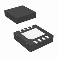
IC CLOCK BUFFER DUAL 40MHZ 8-LLP
Manufacturer
National Semiconductor
Type
Fanout Buffer (Distribution)r
Datasheet
1.LMV112SDNOPB.pdf
(14 pages)
Specifications of LMV112SD/NOPB
Number Of Circuits
2
Ratio - Input:output
2:2
Differential - Input:output
No/No
Input
Clock
Output
Clock
Frequency - Max
40MHz
Voltage - Supply
2.4 V ~ 5.0 V
Operating Temperature
-40°C ~ 85°C
Mounting Type
Surface Mount
Package / Case
8-LLP
Frequency-max
40MHz
Slew Rate
110V/µs
Supply Voltage Range
2.4V To 5V
Logic Case Style
LLP
No. Of Pins
8
Operating Temperature Range
-40°C To +85°C
Msl
MSL 1 - Unlimited
Single Supply Voltage Min (+v)
2.4V
Rohs Compliant
Yes
Amplifier Case Style
LLP
For Use With
LMV112SDEVAL - BOARD EVALUATION FOR LMV112SD
Lead Free Status / RoHS Status
Lead free / RoHS Compliant
Other names
*LMV112SD
LMV112SD
LMV112SDNOPB
LMV112SDNOPBTR
LMV112SDNOPBTR
LMV112SDTR
LMV112SD
LMV112SDNOPB
LMV112SDNOPBTR
LMV112SDNOPBTR
LMV112SDTR
Available stocks
Company
Part Number
Manufacturer
Quantity
Price
Company:

Part Number:
LMV112SD/NOPB
Manufacturer:
TI
Quantity:
144


Application Section
LAYOUT DESIGN RECOMMENDATION
Careful consideration for circuitry design and PCB layout will
eliminate problems and will optimize the performance of the
LMV112. It is best to have the same ground plane on the
PCB for all power supply lines. This gives a low impedance
return path for all decoupling and other ground connections.
To ensure a clean supply voltage it is best to place decou-
pling capacitors close to the LMV112, between V
ground. The output of the VCO must be correctly terminated
with proper load impedance.
(Continued)
CC
and
13
Another important issue is the value of the components,
which also determines the sensitivity to disturbances. Resis-
tor value’s should be but avoid using values that cause a
significant increase in power consumption while loading in-
puts or outputs to heavily.
www.national.com
Related parts for LMV112SD/NOPB
Image
Part Number
Description
Manufacturer
Datasheet
Request
R

Part Number:
Description:
IC,Dual Clock Driver,CMOS,LLCC,8PIN,PLASTIC
Manufacturer:
National Semiconductor
Datasheet:

Part Number:
Description:
National Semiconductor [8-Bit D/A Converter]
Manufacturer:
National Semiconductor
Datasheet:
Part Number:
Description:
National Semiconductor [Media Coprocessor]
Manufacturer:
National Semiconductor
Datasheet:
Part Number:
Description:
Digitally Controlled Tone and Volume Circuit with Stereo Audio Power Amplifier, Microphone Preamp Stage and National 3D Sound
Manufacturer:
National Semiconductor
Datasheet:
Part Number:
Description:
Digitally Controlled Tone and Volume Circuit with Stereo Audio Power Amplifier, Microphone Preamp Stage and National 3D Sound
Manufacturer:
National Semiconductor
Datasheet:
Part Number:
Description:
AC97 Rev 2 Codec with Sample Rate Conversion and National 3D Sound
Manufacturer:
National Semiconductor
Part Number:
Description:
Manufacturer:
National Semiconductor
Datasheet:
Part Number:
Description:
Manufacturer:
National Semiconductor
Datasheet:
Part Number:
Description:
General Purpose, Low Voltage, Low Power, Rail-to-Rail Output Operational Amplifiers
Manufacturer:
National Semiconductor
Datasheet:
Part Number:
Description:
8-bit 20 MSPS flash A/D converter.
Manufacturer:
National Semiconductor
Datasheet:
Part Number:
Description:
Low Noise Quad Operational Amplifier
Manufacturer:
National Semiconductor
Datasheet:
Part Number:
Description:
Quad Differential Line Receivers
Manufacturer:
National Semiconductor
Datasheet:
Part Number:
Description:
Quad High Speed Trapezoidal? Bus Transceiver
Manufacturer:
National Semiconductor
Datasheet:
Part Number:
Description:
Dual Line Receiver
Manufacturer:
National Semiconductor
Datasheet: