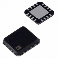
ADCLK925BCPZ-R2 Analog Devices Inc, ADCLK925BCPZ-R2 Datasheet - Page 11

ADCLK925BCPZ-R2
Manufacturer Part Number
ADCLK925BCPZ-R2
Description
IC CLOCK/DATA BUFFER 1:2 16LFCSP
Manufacturer
Analog Devices Inc
Series
SIGer
Type
Fanout Buffer (Distribution), Datar
Datasheet
1.ADCLK905BCPZ-R7.pdf
(16 pages)
Specifications of ADCLK925BCPZ-R2
Number Of Circuits
1
Ratio - Input:output
1:2
Differential - Input:output
Yes/Yes
Input
Clock
Output
ECL, NECL, PECL
Frequency - Max
7.5GHz
Voltage - Supply
2.375 V ~ 3.63 V
Operating Temperature
-40°C ~ 125°C
Mounting Type
Surface Mount
Package / Case
16-LFCSP
Frequency-max
7.5GHz
Clock Ic Type
Clock Buffer
Frequency
7.5GHz
No. Of Outputs
2
Supply Current
77mA
Supply Voltage Range
2.375V To 3.63V
Digital Ic Case Style
LFCSP
No. Of Pins
16
Lead Free Status / RoHS Status
Lead free / RoHS Compliant
For Use With
ADCLK925/PCBZ - BOARD EVAL FOR ADCLK925 16LFCSP
Lead Free Status / RoHS Status
Lead free / RoHS Compliant, Lead free / RoHS Compliant
APPLICATIONS INFORMATION
POWER/GROUND LAYOUT AND BYPASSING
The ADCLK905/ADCLK907/ADCLK925 buffers are designed
for very high speed applications. Consequently, high speed design
techniques must be used to achieve the specified performance.
It is critically important to use low impedance supply planes for
both the negative supply (V
as part of a multilayer board. Providing the lowest inductance
return path for switching currents ensures the best possible
performance in the target application.
It is also important to adequately bypass the input and output
supplies. A 1 μF electrolytic bypass capacitor should be placed
within several inches of each power supply pin to ground. In
addition, multiple high quality 0.001 μF bypass capacitors
should be placed as close as possible to each of the V
supply pins and should be connected to the GND plane with
redundant vias. High frequency bypass capacitors should be
carefully selected for minimum inductance and ESR. Parasitic
layout inductance should be strictly avoided to maximize the
effectiveness of the bypass at high frequencies.
OUTPUT STAGES
The specified performance can be achieved only by using proper
transmission line terminations. The outputs of the ADCLK905/
ADCLK907/ADCLK925 buffers are designed to directly drive
800 mV into 50 Ω cable or microstrip/stripline transmission
lines terminated with 50 Ω referenced to V
output stage is shown in Figure 25. The outputs are designed for
best transmission line matching. If high speed signals must be
routed more than a centimeter, either the microstrip or the
stripline technique is required to ensure proper transition times
and to prevent excessive output ringing and pulse width-
dependent propagation delay dispersion.
the ADCLK905/ADCLK907/ADCLK925 PECL Output Stage
Figure 25. Simplified Schematic Diagram of
V
EE
EE
) and the positive supply (V
V
CC
CC
− 2 V. The PECL
Q
Q
EE
CC
and V
) planes
CC
Rev. 0 | Page 11 of 16
OPTIMIZING HIGH SPEED PERFORMANCE
As with any high speed circuit, proper design and layout
techniques are essential to obtaining the specified performance.
Stray capacitance, inductance, inductive power and ground
impedances, or other layout issues can severely limit performance
and cause oscillation. Discontinuities along input and output
transmission lines can also severely limit the specified jitter
performance by reducing the effective input slew rate.
In a 50 Ω environment, input and output matching have a
significant impact on performance. The buffer provides internal
50 Ω termination resistors for both D and D inputs. The return
side should normally be connected to the reference pin provided.
The termination potential should be carefully bypassed, using
ceramic capacitors to prevent undesired aberrations on the
input signal due to parasitic inductance in the termination
return path. If the inputs are directly coupled to a source, care
must be taken to ensure the pins are within the rated input
differential and common-mode ranges.
If the return is floated, the device exhibits 100 Ω cross termination,
but the source must then control the common-mode voltage
and supply the input bias currents.
There are ESD/clamp diodes between the input pins to prevent
the application of excessive offsets to the input transistors. ESD
diodes are not optimized for best ac performance. When a
clamp is desired, it is recommended that appropriate external
diodes be used.
BUFFER RANDOM JITTER
The ADCLK905/ADCLK907/ADCLK925 are specifically
designed to minimize added random jitter over a wide input
slew rate range. Provided sufficient voltage swing is present,
random jitter is affected most by the slew rate of the input signal.
Whenever possible, excessively large input signals should be
clamped with fast Schottky diodes because attenuators reduce
the slew rate. Input signal runs of more than a few centimeters
should be over low loss dielectrics or cables with good high
frequency characteristics.
ADCLK905/ADCLK907/ADCLK925


