MAX9312ECJ+ Maxim Integrated Products, MAX9312ECJ+ Datasheet - Page 2
MAX9312ECJ+
Manufacturer Part Number
MAX9312ECJ+
Description
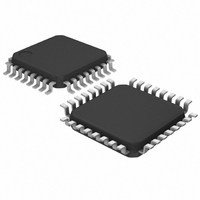
IC DVR CLK/DATA DUAL 1:5 32LQFP
Manufacturer
Maxim Integrated Products
Type
Fanout Buffer (Distribution), Datar
Datasheet
1.MAX9312ETJ.pdf
(9 pages)
Specifications of MAX9312ECJ+
Number Of Circuits
2
Ratio - Input:output
1:5
Differential - Input:output
Yes/Yes
Input
HSTL, LVECL, LVPECL
Output
LVECL, LVPECL
Frequency - Max
3GHz
Voltage - Supply
2.25 V ~ 3.8 V
Operating Temperature
-40°C ~ 85°C
Mounting Type
Surface Mount
Package / Case
32-LQFP
Frequency-max
3GHz
Lead Free Status / RoHS Status
Lead free / RoHS Compliant


ABSOLUTE MAXIMUM RATINGS
V
Inputs (CLK_, CLK_) .............................V
CLK_ to CLK_ ....................................................................±3.0V
Continuous Output Current .................................................50mA
Surge Output Current........................................................100mA
V
Continuous Power Dissipation (T
Junction-to-Case Thermal Resistance (T
DC ELECTRICAL CHARACTERISTICS
(V
Dual 1:5 Differential LVPECL/LVECL/HSTL
Clock and Data Drivers
Note 1: Package thermal resistances were obtained using the method described in JEDEC specification JESD51-7, using a four-
Stresses beyond those listed under “Absolute Maximum Ratings” may cause permanent damage to the device. These are stress ratings only, and functional
operation of the device at these or any other conditions beyond those indicated in the operational sections of the specifications is not implied. Exposure to
absolute maximum rating conditions for extended periods may affect device reliability.
2
PARAMETER
INPUTS (CLK_, CLK _ )
Single-Ended
Input High
Voltage
Single-Ended
Input Low
Voltage
High Voltage of
Differential Input
Low Voltage of
Differential Input
Differential Input
Voltage
Input High
Current
CLK_ Input Low
Current
CC
BB
CC
32-Pin LQFP (derate 20.7mW/°C above +70°C) ....1652.9mW
32-Pin TQFN (derate 34.5mW/°C above +70°C)....2758.6mW
32-Pin LQFP ................................................................12°C/W
32-Pin TQFN ..................................................................2°C/W
_______________________________________________________________________________________
Sink/Source Current ...............................................±0.65mA
- V
- V
EE
EE
layer board. For detailed information on package thermal considerations, refer to www.maxim-ic.com/thermal-tutorial.
...............................................................................4.1V
= +2.25V to +3.8V, outputs loaded with 50Ω ±1% to V
SYMBOL
V
I
V
ILCLK
V
V
V
IHD
V
I
IHD
ILD
ILD
IH
IH
IL
-
V
connected
to CLK_
(V
connected
to C LK_)
V
connected
to CLK_
(V
connected
to C LK_)
For V
For V
B B
B B
A
IL
IL
= +70°C)
CONDITIONS
for V
for V
CC
CC
- V
- V
B B
B B
JC
EE
EE
EE
) (Note A)
- 0.3V to V
MAX9312
MAX9314
MAX9312
MAX9314
< 3.0V
≥ 3.0V
CC
+ 0.3V
V
V
V
1.165
0.095
0.095
MIN
1.23
V
V
V
-10
EE
1.2
CC
CC
EE
EE
EE
+
-
-
-40°C
CC
MAX
- 2V.) (Notes 2–5)
V
V
1.475
V
0.095
V
1.62
V
V
V
+10
V
150
Junction-to-Ambient Thermal Resistance (T
Operating Temperature Range ...........................-40°C to +85°C
Junction Temperature ......................................................+150°C
Storage Temperature Range .............................-65°C to +150°C
ESD Protection
Soldering Temperature (10s) ...........................................+300°C
3.0
CC
CC
CC
CC
CC
CC
CC
EE
Human Body Model (CLK_, CLK_, Q_, Q_) ........................2kV
32-Pin LQFP .............................................................48.4°C/W
32-Pin TQFN ................................................................29°C/W
-
-
-
-
V
V
V
1.165
0.095
0.095
MIN
1.23
V
V
V
EE
1.2
-10
CC
CC
EE
EE
EE
+
+25°C
-
-
MAX
V
V
1.475
V
0.095
V
V
V
1.62
V
V
+10
150
3.0
CC
CC
CC
CC
CC
CC
CC
EE
-
-
-
-
V
MIN
V
V
1.165
0.095
0.095
1.23
V
V
V
-10
EE
1.2
CC
CC
EE
EE
EE
+
+85°C
-
-
JA
MAX
V
V
1.475
V
0.095
V
V
V
1.62
V
V
+10
) (Note 1)
150
3.0
CC
CC
CC
CC
CC
CC
CC
EE
-
-
-
-
UNITS
µA
µA
V
V
V
V
V
Related parts for MAX9312ECJ+
Image
Part Number
Description
Manufacturer
Datasheet
Request
R

Part Number:
Description:
Manufacturer:
Maxim Integrated Products
Datasheet:

Part Number:
Description:
Ultra Low-Power, Low-Cost Comparators with 2eference
Manufacturer:
MAXIM [Maxim Integrated Products]
Datasheet:
Part Number:
Description:
MAX7528KCWPMaxim Integrated Products [CMOS Dual 8-Bit Buffered Multiplying DACs]
Manufacturer:
Maxim Integrated Products
Datasheet:
Part Number:
Description:
Single +5V, fully integrated, 1.25Gbps laser diode driver.
Manufacturer:
Maxim Integrated Products
Datasheet:
Part Number:
Description:
Single +5V, fully integrated, 155Mbps laser diode driver.
Manufacturer:
Maxim Integrated Products
Datasheet:
Part Number:
Description:
VRD11/VRD10, K8 Rev F 2/3/4-Phase PWM Controllers with Integrated Dual MOSFET Drivers
Manufacturer:
Maxim Integrated Products
Datasheet:
Part Number:
Description:
Highly Integrated Level 2 SMBus Battery Chargers
Manufacturer:
Maxim Integrated Products
Datasheet:
Part Number:
Description:
Current Monitor and Accumulator with Integrated Sense Resistor; ; Temperature Range: -40°C to +85°C
Manufacturer:
Maxim Integrated Products
Part Number:
Description:
TSSOP 14/A°/RS-485 Transceivers with Integrated 100O/120O Termination Resis
Manufacturer:
Maxim Integrated Products
Part Number:
Description:
TSSOP 14/A°/RS-485 Transceivers with Integrated 100O/120O Termination Resis
Manufacturer:
Maxim Integrated Products
Part Number:
Description:
QFN 16/A°/AC-DC and DC-DC Peak-Current-Mode Converters with Integrated Step
Manufacturer:
Maxim Integrated Products
Part Number:
Description:
TDFN/A/65V, 1A, 600KHZ, SYNCHRONOUS STEP-DOWN REGULATOR WITH INTEGRATED SWI
Manufacturer:
Maxim Integrated Products
Part Number:
Description:
Integrated Temperature Controller f
Manufacturer:
Maxim Integrated Products
Part Number:
Description:
SOT23-6/I°/45MHz to 650MHz, Integrated IF VCOs with Differential Output
Manufacturer:
Maxim Integrated Products
Part Number:
Description:
SOT23-6/I°/45MHz to 650MHz, Integrated IF VCOs with Differential Output
Manufacturer:
Maxim Integrated Products