NB4N121KMNG ON Semiconductor, NB4N121KMNG Datasheet
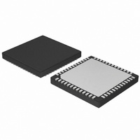
IC FANOUT CLK DRVR HCSL 52-QFN

NB4N121KMNG

Manufacturer Part Number
NB4N121KMNG
Description
IC FANOUT CLK DRVR HCSL 52-QFN
Manufacturer
ON Semiconductor
Type
Fanout Buffer (Distribution)r
Datasheet

Specifications of NB4N121KMNG

Number Of Circuits
1
Ratio - Input:output
1:21
Differential - Input:output
Yes/Yes
Input
CML, LVCMOS, LVDS, LVPECL, LVTTL
Output
HCSL
Frequency - Max
400MHz
Voltage - Supply
3 V ~ 3.6 V
Operating Temperature
-40°C ~ 70°C
Mounting Type
Surface Mount
Package / Case
52-VFQFN Exposed Pad
Frequency-max
400MHz
Lead Free Status / RoHS Status
Lead free / RoHS Compliant

Available stocks

Company
Part Number
Manufacturer
Quantity
Price
Part Number:
NB4N121KMNG
Manufacturer:
ON Semiconductor
Quantity:
95
Part Number:
NB4N121KMNG
Manufacturer:
ON/安森美
Quantity:
20 000
NB4N121K
3.3V Differential In 1:21
Differential Fanout Clock
Driver with HCSL level
Output
Description
21 HCSL level differential outputs, optimized for ultra low
propagation delay variation. The NB4N121K is designed with HCSL
clock distribution for FBDIMM applications in mind.
Single−ended LVPECL, CML, LVCMOS or LVTTL levels are
accepted with the proper V
and 13). Clock input pins incorporate an internal 50 W on die
termination resistors.
connecting to GND. To drive a 2X load, connect I
Figure 9.
skews. Optimal design, layout, and processing minimize skew within
a device and from device to device. System designers can take
advantage of the NB4N121K’s performance to distribute low skew
clocks across the backplane or the motherboard.
Features
*For additional information on our Pb−Free strategy and soldering details, please
© Semiconductor Components Industries, LLC, 2010
February, 2010 − Rev. 4
download the ON Semiconductor Soldering and Mounting Techniques
Reference Manual, SOLDERRM/D.
The NB4N121K is a Clock differential input fanout distribution 1 to
Inputs can accept differential LVPECL, CML, or LVDS levels.
Output drive current at I
The NB4N121K specifically guarantees low output–to–output
400 MHz
Differential Pair
Typical Input Clock Frequency 100, 133, 166, 200, 266, 333 and
340 ps Typical Rise and Fall Times
800 ps Typical Propagation Delay
Dtpd 100 ps Maximum Propagation Delay Variation Per Each
<1 ps RMS Additive Clock jitter
Operating Range: V
Differential HCSL Output Level (700 mV Peak−to−Peak)
Pb−Free Packages are Available*
CC
= 3.0 V to 3.6 V with V
REFAC
REF
(Pin 1) for 1X load is selected by
supply (see Figures 5, 10, 11, 12,
EE
REF
= 0 V
to V
1
CC
. See
See detailed ordering and shipping information in the package
dimensions section on page 8 of this data sheet.
VTCLK
VTCLK
CLK
CLK
GND
Figure 1. Pin Configuration (Top View)
V
*For additional marking information, refer to
Application Note AND8002/D.
CC
ORDERING INFORMATION
A
WL
YY
WW
G
MARKING DIAGRAM*
1
http://onsemi.com
1
52
52
AWLYYWWG
= Assembly Site
= Wafer Lot
= Year
= Work Week
= Pb−Free Package
NB4N
121K
Publication Order Number:
R
REF
CASE 485M
MN SUFFIX
QFN−52
NB4N121K/D
I
REF
Q19
Q19
Q20
Q20
Q0
Q0
Q1
Q1

Related parts for NB4N121KMNG

NB4N121KMNG Summary of contents

Page 1

... Differential HCSL Output Level (700 mV Peak−to−Peak) • Pb−Free Packages are Available* *For additional information on our Pb−Free strategy and soldering details, please download the ON Semiconductor Soldering and Mounting Techniques Reference Manual, SOLDERRM/D. © Semiconductor Components Industries, LLC, 2010 February, 2010 − Rev ...

Page 2

I 1 REF GND 2 VTCLK 3 CLK 4 5 CLK VTCLK Q20 8 9 Q20 10 Q19 Q19 11 12 Q18 13 Q18 Table 1. PIN DESCRIPTION Pin Name 1 I REF 2 GND 3, ...

Page 3

Table 2. ATTRIBUTES Input Default State Resistors ESD Protection Moisture Sensitivity (Note 2) Flammability Rating Oxygen Index Transistor Count Meets or exceeds JEDEC Spec EIA/JESD78 IC Latchup Test 2. For additional information, see Application Note AND8003/D. Table ...

Page 4

Table 4. DC CHARACTERISTICS (V Symbol I GND Supply Current (All Outputs Loaded) GND I Power Supply Current (All Outputs Loaded Input HIGH Current CLKx, CLKx IH I Input LOW Current CLKx, CLKx IL DIFFERENTIAL INPUT DRIVEN SINGLE−ENDED ...

Page 5

Table 5. AC CHARACTERISTICS V Symbol V Output Voltage Amplitude (@ V OUTPP t , Propagation Delay to (See Figure 3) PLH t PHL Dt , Propagation Delay Variations Variation Per Each Diff Pair CLK/CLK to Qx/Qx (Note 8) PLH ...

Page 6

V CROSS 175 mV Figure 4. HCSL Output Parameter Characteristics CLK V th CLK V th Figure 5. Differential Input Driven Single−Ended ( REFAC thmax IHmax V ILmax ...

Page 7

HCSL Driver REF A. For 1X configuration, connect pin IREF to GND or for 2X configuration, connect pin to V ...

Page 8

... Internal Input Termination Resistor Figure 12. Standard 50 W Load CML Interface INTQ ORDERING INFORMATION Device NB4N121KMN NB4N121KMNG NB4N121KMNR2 NB4N121KMNR2G †For information on tape and reel specifications, including part orientation and tape sizes, please refer to our Tape and Reel Packaging Specifications Brochure, BRD8011/D. V ...

Page 9

... Opportunity/Affirmative Action Employer. This literature is subject to all applicable copyright laws and is not for resale in any manner. PUBLICATION ORDERING INFORMATION LITERATURE FULFILLMENT: Literature Distribution Center for ON Semiconductor P.O. Box 5163, Denver, Colorado 80217 USA Phone: 303−675−2175 or 800−344−3860 Toll Free USA/Canada Fax: 303− ...

Related keywords