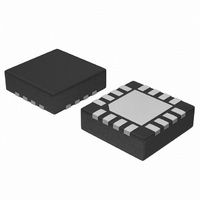
NB6N14SMNG ON Semiconductor, NB6N14SMNG Datasheet - Page 2

NB6N14SMNG
Manufacturer Part Number
NB6N14SMNG
Description
IC CLK/DATA RCVR DIFF 1:4 16-QFN
Manufacturer
ON Semiconductor
Series
AnyLevel™ ECLinPS MAX™r
Type
Fanout Buffer (Distribution), Translatorr
Datasheet
1.NB6N14SMNR2G.pdf
(11 pages)
Specifications of NB6N14SMNG
Number Of Circuits
1
Ratio - Input:output
1:4
Differential - Input:output
Yes/Yes
Input
CML, LVDS, LVPECL
Output
LVDS
Frequency - Max
2GHz
Voltage - Supply
3 V ~ 3.6 V
Operating Temperature
-40°C ~ 85°C
Mounting Type
Surface Mount
Package / Case
16-TFQFN Exposed Pad
Frequency-max
2GHz
Number Of Outputs
8
Max Input Freq
2000 MHz (Min)
Propagation Delay (max)
0.6 ns @ 3V to 3.6V
Supply Voltage (max)
3.6 V
Supply Voltage (min)
3 V
Maximum Operating Temperature
+ 85 C
Minimum Operating Temperature
- 40 C
Mounting Style
SMD/SMT
Lead Free Status / RoHS Status
Lead free / RoHS Compliant
Other names
NB6N14SMNG
NB6N14SMNGOS
NB6N14SMNGOS
Available stocks
Company
Part Number
Manufacturer
Quantity
Price
Company:
Part Number:
NB6N14SMNG
Manufacturer:
ON
Quantity:
760
Company:
Part Number:
NB6N14SMNG
Manufacturer:
ON
Quantity:
298
2. In the differential configuration, when the input termination pin (VT) is connected to a termination voltage or left open, and if no signal is applied
Table 2. PIN DESCRIPTION
on IN/IN inputs, then the device will be susceptible to self−oscillation.
Pin
Figure 3. NB6N14S Pinout, 16−pin QFN
10
11
12
13
14
15
16
1
2
3
4
5
6
7
8
9
−
Q1
Q1
Q2
Q2
1
2
3
4
V
Name
REF_AC
GND
V
V
EN
Q1
Q1
Q2
Q2
Q3
Q3
Q0
Q0
EP
V
IN
IN
CC
CC
T
Q3
Q0
16
5
NB6N14S
Q0
15
Q3
6
LVTTL / LVCMOS Input
LVPECL, CML, LVDS
LVPECL, CML, LVDS
V
V
LVPECL Output
LVPECL Output
14
7
LVDS Output
LVDS Output
LVDS Output
LVDS Output
LVDS Output
LVDS Output
LVDS Output
LVDS Output
CC
CC
GND
I/O
13
EN
8
−
−
−
−
12
11
10
9
(Top View)
IN
V
V
IN
Exposed Pad (EP)
T
REF_AC
http://onsemi.com
Non−inverted IN output. Typically loaded with 100 W receiver termination
resistor across differential pair.
Inverted IN output. Typically loaded with 100 W receiver termination resistor
across differential pair.
Non−inverted IN output. Typically loaded with 100 W receiver termination
resistor across differential pair.
Inverted IN output. Typically loaded with 100 W receiver termination resistor
across differential pair.
Non−inverted IN output. Typically loaded with 100 W receiver termination
resistor across differential pair.
Inverted IN output. Typically loaded with 100 W receiver termination resistor
across differential pair.
Positive Supply Voltage.
Synchronous Output Enable. When LOW, Q outputs will go LOW and Qb
outputs will go HIGH on the next negative transition of IN input. The internal
DFF register is clocked on the falling edge of IN input; see Figure 23. The EN
pin has an internal pullup resistor and defaults HIGH when left open.
Inverted Differential Input
The V
differential or single−ended input signals. For the capacitor−coupled IN and/or
INb inputs, V
ground with a 0.01 mF capacitor.
Internal 100 W Center−tapped Termination Pin for IN and IN
Non−inverted Differential Input. (Note 2)
Negative Supply Voltage.
Positive Supply Voltage.
Non−inverted IN output. Typically loaded with 100 W receiver termination
resistor across differential pair.
Inverted IN output. Typically loaded with 100 W receiver termination resistor
across differential pair.
The Exposed Pad (EP) on the QFN−16 package bottom is thermally connected
to the die for improved heat transfer out of package. The exposed pad must be
attached to a heat−sinking conduit. The pad is not electrically connected to the
die, but is recommended to be electrically and thermally connected to GND on
the PC board.
REF_AC
2
Table 1. TRUTH TABLE
1. On next transition of the input signal (IN).
REF_AC
reference output can be used to rebias capacitor−coupled
IN
0
1
x
should be connected to the VT pin and bypassed to
IN
1
0
x
Description
EN
1
1
0
0 (Note 1)
Q
0
1
1 (Note 1)
Q
1
0


